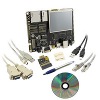
BMSKTOPASA900(DCE) Toshiba, BMSKTOPASA900(DCE) Datasheet - Page 24

BMSKTOPASA900(DCE)
Manufacturer Part Number
BMSKTOPASA900(DCE)
Description
KIT STARTER TMPA900 USB JTAG
Manufacturer
Toshiba
Series
TOPASr
Type
MCUr
Specifications of BMSKTOPASA900(DCE)
Contents
Evaluation Board, Cable(s), Software and Documentation
For Use With/related Products
TMPA900CMXBG
Lead Free Status / RoHS Status
Lead free / RoHS Compliant
- Current page: 24 of 959
- Download datasheet (5Mb)
Pin Functions and Initial Values Arranged by Type of Power Supply – 2 (DVCCM)
Power supply to
DVCCM
be used
Note 1:
Note 2:
Typical pin name
PR0
PR1
PR2
SL0
SL1
SL2
SL4
SL5
SL6
Pin names "SA0 through SA7, …, and SU0 through SU4" are symbols used for convenience and are
different from general-purpose port functions "PA0 through PA7, …, and PV0 through PV7."
When the “Input buffer” column shows “ON”, the pin is enabled as an input in the initial state. If necessary,
the pin should be processed externally. When DDR SDRAM is used, the DQS signals (DMCDDQS0,
DMCDDQS1) are always enabled as inputs. These pins must be tied externally (pulled up/down, etc.) to
prevent flow-through current.
-
-
RESETOUTn
DMCDDQS0
DMCDDQS1
DMCDCLKN
DMCCLKIN
DMCSCLK
Alternative
DMCAP
function
FCOUT
INTH
TENTATIVE
TMPA900CM- 23
DMCDCLKP
Alternative
OFDOUTn
function
-
-
-
-
-
-
-
up/down
Pull
-
-
-
-
-
-
-
-
-
buffer
Input
ON
ON
ON
ON
-
-
-
-
-
When SELMEMC = 0
When SELMEMC = 1
When SELMEMC = 0
When SELMEMC = 1
DMCAP out / “L” output
OFDOUTn out / “H” output
DMCDDQS0 / Hz*
DMCDDQS1 / Hz*
DMCCLKIN input / Hz
RESETOUTn output /
INTH Input / Hz
DMCDCLKN out /Inverted CLK output
DMCSCLK out / CLK output
DMCDCLKP out / CLK output
Invalid signal/ “H” output
During reset: “L” output
After reset: “H” output
Initial value after reset
function/pin state
TMPA900CM
2009-10-14
Related parts for BMSKTOPASA900(DCE)
Image
Part Number
Description
Manufacturer
Datasheet
Request
R
Part Number:
Description:
Toshiba Semiconductor [TOSHIBA IGBT Module Silicon N Channel IGBT]
Manufacturer:
TOSHIBA Semiconductor CORPORATION
Datasheet:
Part Number:
Description:
TOSHIBA GTR MODULE SILICON NPN TRIPLE DIFFUSED TYPE
Manufacturer:
TOSHIBA Semiconductor CORPORATION
Datasheet:
Part Number:
Description:
TOSHIBA GTR Module Silicon N Channel IGBT
Manufacturer:
TOSHIBA Semiconductor CORPORATION
Datasheet:
Part Number:
Description:
TOSHIBA Intelligent Power Module Silicon N Channel IGBT
Manufacturer:
TOSHIBA Semiconductor CORPORATION
Datasheet:
Part Number:
Description:
TOSHIBA INTELLIGENT POWER MODULE SILICON N CHANNEL LGBT
Manufacturer:
TOSHIBA Semiconductor CORPORATION
Datasheet:
Part Number:
Description:
TOSHIBA IGBT Module Silicon N Channel IGBT
Manufacturer:
TOSHIBA Semiconductor CORPORATION
Datasheet:
Part Number:
Description:
TOSHIBA GTR MODULE SILICON N−CHANNEL IGBT
Manufacturer:
TOSHIBA Semiconductor CORPORATION
Datasheet:
Part Number:
Description:
TOSHIBA Intelligent Power Module Silicon N Channel IGBT
Manufacturer:
TOSHIBA Semiconductor CORPORATION
Datasheet:
Part Number:
Description:
TOSHIBA GTR Module Silicon N Channel IGBT
Manufacturer:
TOSHIBA Semiconductor CORPORATION
Datasheet:
Part Number:
Description:
TOSHIBA INTELLIGENT POWER MODULE
Manufacturer:
TOSHIBA Semiconductor CORPORATION
Datasheet:
Part Number:
Description:
TOSHIBA Intelligent Power Module Silicon N Channel IGBT
Manufacturer:
TOSHIBA Semiconductor CORPORATION
Datasheet:
Part Number:
Description:
TOSHIBA Intelligent Power Module Silicon N Channel IGBT
Manufacturer:
TOSHIBA Semiconductor CORPORATION
Datasheet:
Part Number:
Description:
TOSHIBA IGBT Module Silicon N Channel IGBT
Manufacturer:
TOSHIBA Semiconductor CORPORATION
Datasheet:
Part Number:
Description:
TOSHIBA Intelligent Power Module Silicon N Channel IGBT
Manufacturer:
TOSHIBA Semiconductor CORPORATION
Datasheet:
Part Number:
Description:
Toshiba Semiconductor [SILICON N CHANNEL 1GBT]
Manufacturer:
TOSHIBA Semiconductor CORPORATION
Datasheet:


