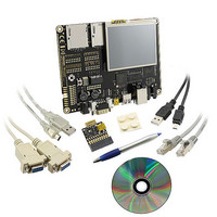
BMSKTOPASA900(DCE) Toshiba, BMSKTOPASA900(DCE) Datasheet - Page 51

BMSKTOPASA900(DCE)
Manufacturer Part Number
BMSKTOPASA900(DCE)
Description
KIT STARTER TMPA900 USB JTAG
Manufacturer
Toshiba
Series
TOPASr
Type
MCUr
Specifications of BMSKTOPASA900(DCE)
Contents
Evaluation Board, Cable(s), Software and Documentation
For Use With/related Products
TMPA900CMXBG
Lead Free Status / RoHS Status
Lead free / RoHS Compliant
- Current page: 51 of 959
- Download datasheet (5Mb)
RESETn AM1 AM0
Mode setting pin
Mode setting pin
Mode setting pin
3.3.1
SELMEMC
1.
2.
3.
4.
SELVCCM
SELJTAG
Mode setting pin
Boot memory setting
External memory voltage setting (Except NANDF)
External memory controller setting
JTAG pin setting
0
1
0
1
0
1
0
1
1
0
external pin setting.
Boot mode
A few boot modes are available for choice to this microprocessor depending on the
1
0
1
0
Memory-related control pins operate at 1.8±0.1V (DVCCM)
Memory-related control pins operate at 3.3±0.3V (DVCCM)
Only the SDR (Single Data Rate) and Mobile SDR types of SDRAM can be used.
Only the Mobile DDR (Mobile Double Data Rate) type of SDRAM can be used.
Set “0” to this pin except Boundary Scan Mode.
This setting can be used as regular Debug Mode
Note: Debugging cannot be carried out during internal BOOT with AM1 = 1 and AM0 = 1.
This setting can be used as Boundary Scan Mode
Start from the external 16-bit NOR Flash memory
(Internal BOOT_TOM cannot be seen)
Start from the external 32-bit NOR Flash memory
(Internal BOOT_TOM cannot be seen)
BOOT (start from the Internal boot ROM)
BOOT (start from the Internal boot ROM)
TEST (this setting cannot be used)
TENTATIVE
TMPA900CM- 50
Operation mode
Operation mode
Operation mode
Operation mode
TMPA900CM
2009-10-14
Related parts for BMSKTOPASA900(DCE)
Image
Part Number
Description
Manufacturer
Datasheet
Request
R
Part Number:
Description:
Toshiba Semiconductor [TOSHIBA IGBT Module Silicon N Channel IGBT]
Manufacturer:
TOSHIBA Semiconductor CORPORATION
Datasheet:
Part Number:
Description:
TOSHIBA GTR MODULE SILICON NPN TRIPLE DIFFUSED TYPE
Manufacturer:
TOSHIBA Semiconductor CORPORATION
Datasheet:
Part Number:
Description:
TOSHIBA GTR Module Silicon N Channel IGBT
Manufacturer:
TOSHIBA Semiconductor CORPORATION
Datasheet:
Part Number:
Description:
TOSHIBA Intelligent Power Module Silicon N Channel IGBT
Manufacturer:
TOSHIBA Semiconductor CORPORATION
Datasheet:
Part Number:
Description:
TOSHIBA INTELLIGENT POWER MODULE SILICON N CHANNEL LGBT
Manufacturer:
TOSHIBA Semiconductor CORPORATION
Datasheet:
Part Number:
Description:
TOSHIBA IGBT Module Silicon N Channel IGBT
Manufacturer:
TOSHIBA Semiconductor CORPORATION
Datasheet:
Part Number:
Description:
TOSHIBA GTR MODULE SILICON N−CHANNEL IGBT
Manufacturer:
TOSHIBA Semiconductor CORPORATION
Datasheet:
Part Number:
Description:
TOSHIBA Intelligent Power Module Silicon N Channel IGBT
Manufacturer:
TOSHIBA Semiconductor CORPORATION
Datasheet:
Part Number:
Description:
TOSHIBA GTR Module Silicon N Channel IGBT
Manufacturer:
TOSHIBA Semiconductor CORPORATION
Datasheet:
Part Number:
Description:
TOSHIBA INTELLIGENT POWER MODULE
Manufacturer:
TOSHIBA Semiconductor CORPORATION
Datasheet:
Part Number:
Description:
TOSHIBA Intelligent Power Module Silicon N Channel IGBT
Manufacturer:
TOSHIBA Semiconductor CORPORATION
Datasheet:
Part Number:
Description:
TOSHIBA Intelligent Power Module Silicon N Channel IGBT
Manufacturer:
TOSHIBA Semiconductor CORPORATION
Datasheet:
Part Number:
Description:
TOSHIBA IGBT Module Silicon N Channel IGBT
Manufacturer:
TOSHIBA Semiconductor CORPORATION
Datasheet:
Part Number:
Description:
TOSHIBA Intelligent Power Module Silicon N Channel IGBT
Manufacturer:
TOSHIBA Semiconductor CORPORATION
Datasheet:
Part Number:
Description:
Toshiba Semiconductor [SILICON N CHANNEL 1GBT]
Manufacturer:
TOSHIBA Semiconductor CORPORATION
Datasheet:


