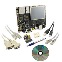
BMSKTOPASA900(DCE) Toshiba, BMSKTOPASA900(DCE) Datasheet - Page 419

BMSKTOPASA900(DCE)
Manufacturer Part Number
BMSKTOPASA900(DCE)
Description
KIT STARTER TMPA900 USB JTAG
Manufacturer
Toshiba
Series
TOPASr
Type
MCUr
Specifications of BMSKTOPASA900(DCE)
Contents
Evaluation Board, Cable(s), Software and Documentation
For Use With/related Products
TMPA900CMXBG
Lead Free Status / RoHS Status
Lead free / RoHS Compliant
- Current page: 419 of 959
- Download datasheet (5Mb)
I2CINT0
Interrupt request
Write to I2C0DBR
I2C0DA pin
I2C0CL pin
<PIN>
3. 1-Word Data Transfer
and determine whether master or slave mode is selected.
(1) When I2C0SR<MST> = 1 (Master mode)
Check I2C0SR<MST> in the interrupt routine after a 1-word data transfer is completed,
Figure 3.14.6 When I2C0CR1<BC> = 0y000 and I2C0CR1<ACK> = 1
I2C0SR<LRB> is 0, the receiver is requesting the next data. Write the data to be
transmitted to I2C0DBR.
I2C0CR1<ACK> to 1, and then write the data to be transmitted to I2C0DBR.
generated to transmit from I2C0CL the data from I2C0DA.
I2C0SR<PIN> is cleared to 0 and I2C0CL is pulled low. If more than one word of data
needs to be transferred, repeat the procedure by checking I2C0SR<LRB>.
condition should be generated to terminate the data transfer.
for 1-word transfer and acknowledge to be output.
operation, read the received data from I2C0DBR.
I2C0CR1<ACK> to 1 and then write dummy data (0x00) to I2C0DBR or set
I2C0CR2<PIN> to 1.
a. When I2C0SR<TRX>=1 (Transmitter mode)
b. When I2C0SR<TRX> = 0 (Receiver mode)
Check I2C0SR<TRX> to determine whether transmitter or receiver mode is selected.
Check the acknowledge status from the receiver with the I2C0SR<LRB> flag. When
If it is necessary to change the transfer data size, change I2C0CR1<BC>, set
After the transmit data is written, I2C0SR<PIN> is set to 1 and serial clocks are
After the transmission is completed, an I2CINT0 interrupt request is generated.
When I2C0SR<LRB> is 1, the receiver is not requesting the next data, so a stop
Writing dummy data (0x00) to I2C0DBR or setting I2C0CR2<PIN> to 1 causes clocks
After an I2CINT0 interrupt request is generated to indicate the end of receive
If it is necessary to change the receive data size, change I2C0CR1<BC>, set
(The data that is read immediately after slave address transmission is undefined.)
D7
1
D6
2
D5
3
TENTATIVE
TMPA900CM- 418
D4
4
D3
5
D2
6
D1
7
D0
8
ACK
Master output
Slave output
9
TMPA900CM
Acknowledge
signal from
Receiver
2009-10-14
Related parts for BMSKTOPASA900(DCE)
Image
Part Number
Description
Manufacturer
Datasheet
Request
R
Part Number:
Description:
Toshiba Semiconductor [TOSHIBA IGBT Module Silicon N Channel IGBT]
Manufacturer:
TOSHIBA Semiconductor CORPORATION
Datasheet:
Part Number:
Description:
TOSHIBA GTR MODULE SILICON NPN TRIPLE DIFFUSED TYPE
Manufacturer:
TOSHIBA Semiconductor CORPORATION
Datasheet:
Part Number:
Description:
TOSHIBA GTR Module Silicon N Channel IGBT
Manufacturer:
TOSHIBA Semiconductor CORPORATION
Datasheet:
Part Number:
Description:
TOSHIBA Intelligent Power Module Silicon N Channel IGBT
Manufacturer:
TOSHIBA Semiconductor CORPORATION
Datasheet:
Part Number:
Description:
TOSHIBA INTELLIGENT POWER MODULE SILICON N CHANNEL LGBT
Manufacturer:
TOSHIBA Semiconductor CORPORATION
Datasheet:
Part Number:
Description:
TOSHIBA IGBT Module Silicon N Channel IGBT
Manufacturer:
TOSHIBA Semiconductor CORPORATION
Datasheet:
Part Number:
Description:
TOSHIBA GTR MODULE SILICON N−CHANNEL IGBT
Manufacturer:
TOSHIBA Semiconductor CORPORATION
Datasheet:
Part Number:
Description:
TOSHIBA Intelligent Power Module Silicon N Channel IGBT
Manufacturer:
TOSHIBA Semiconductor CORPORATION
Datasheet:
Part Number:
Description:
TOSHIBA GTR Module Silicon N Channel IGBT
Manufacturer:
TOSHIBA Semiconductor CORPORATION
Datasheet:
Part Number:
Description:
TOSHIBA INTELLIGENT POWER MODULE
Manufacturer:
TOSHIBA Semiconductor CORPORATION
Datasheet:
Part Number:
Description:
TOSHIBA Intelligent Power Module Silicon N Channel IGBT
Manufacturer:
TOSHIBA Semiconductor CORPORATION
Datasheet:
Part Number:
Description:
TOSHIBA Intelligent Power Module Silicon N Channel IGBT
Manufacturer:
TOSHIBA Semiconductor CORPORATION
Datasheet:
Part Number:
Description:
TOSHIBA IGBT Module Silicon N Channel IGBT
Manufacturer:
TOSHIBA Semiconductor CORPORATION
Datasheet:
Part Number:
Description:
TOSHIBA Intelligent Power Module Silicon N Channel IGBT
Manufacturer:
TOSHIBA Semiconductor CORPORATION
Datasheet:
Part Number:
Description:
Toshiba Semiconductor [SILICON N CHANNEL 1GBT]
Manufacturer:
TOSHIBA Semiconductor CORPORATION
Datasheet:


