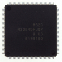
M30845FJGP#U3 Renesas Electronics America, M30845FJGP#U3 Datasheet - Page 77

M30845FJGP#U3
Manufacturer Part Number
M30845FJGP#U3
Description
IC M32C MCU FLASH 512K 144LQFP
Manufacturer
Renesas Electronics America
Series
M16C™ M32C/80r
Specifications of M30845FJGP#U3
Core Processor
M32C/80
Core Size
16/32-Bit
Speed
32MHz
Connectivity
CAN, I²C, IEBus, SIO, UART/USART
Peripherals
DMA, PWM, WDT
Number Of I /o
121
Program Memory Size
512KB (512K x 8)
Program Memory Type
FLASH
Ram Size
24K x 8
Voltage - Supply (vcc/vdd)
3 V ~ 5.5 V
Data Converters
A/D 34x10b, D/A 2x8b
Oscillator Type
Internal
Operating Temperature
-40°C ~ 85°C
Package / Case
144-LQFP
Lead Free Status / RoHS Status
Lead free / RoHS Compliant
Eeprom Size
-
Available stocks
Company
Part Number
Manufacturer
Quantity
Price
- Current page: 77 of 531
- Download datasheet (4Mb)
M
R
R
6.2 Cold Start-up / Warm Start-up Determine Function
e
E
3
. v
J
2
Figure 6.7
Figure 6.8 Cold Start-up/Warm Start-up Determine Function Operation
0
C
6.1.1 Limitations on Exiting Stop/Wait Mode
The WDC5 bit in the WDC register determines either cold start-up, power-on reset, or warm start-up, reset
during the microcomputer running. Default value of the WDC5 bit is "0" (cold start-up) when power-on. It is
set to "1" (warm start-up) by writing desired values to the WDC register. The WDC5 bit is not reset,
regardless of a software reset or reset signal input.
Figure 6.7 shows a block diagram of the cold start-up/warm start-up determine function. Figure 6.8 shows
its operation exmaple.
1
9
0 .
8 /
B
The low voltage detection interrupt is generated and the microcomputer exits stop mode as soon as the
CM10 bit in the CM1 register is set to "1" (all clocks stopped) under the conditions below. Additionally, if
WAIT instruction is executed under these same conditions, the low voltage detection interrupt is immedi-
ately generated and the microcomputer exits wait mode.
- the VC27 bit in the VCR2 register is set to "1" (low voltage detection circuit enabled),
- the D40 bit in the D4INT register is set to "1" (low voltage detection interrupt enabled),
- the D41 bit in the D4INT register is set to "1" (low voltage detection interrupt is used to exit stop/wait
- the voltage applied to the V
Set the CM10 bit to "1" when the VC13 bit is "0" (V
wait mode when the voltage applied to the V
the voltage applied rises to Vdet4 or above.
0
1
4
mode), and
0
3
G
J
6
u
WDC5 Bit
o r
0 -
RESET
. l
u
0
1
V
p
, 7
0
CC1
1
(
Cold Start-up/Warm Start-up Determine Function Block Diagram
Write to WDC register
2
M
0
3
0
"1"
"0"
5V
0V
5V
0V
2
5
C
Hardware Reset 1 when Power-on
NOTES:
8 /
Page 54
, 4
1. Time difference between T1 and T2 may affect the WDC5 bit setting period.
M
3
2
C
Reset Sequence (Approx. 20 s @16MHz)
T1
f o
8 /
T2
CC1
4
4
) T
9
5
pin is higher than Vdet4 (the VC13 bit in the VCR1 register is set to "1")
Pch
CPU reset release
Program running started
T > 100 s
transistor
Set to "1" by program
CC1
ON (Approx. 4V)
pin drops below Vdet4 and to exit stop/wait mode when
WDC5 Bit
CC1
S
R
< Vdet4), if the microcomputer is set to enter stop/
Q
No change
voltage applied
to RESET is 0V.
even if the
(Cold Start-up/Warm Start-up)
COLD/WARM
The WDC5 bit is set to "0"
as soon as enough voltage
is applied to V
6. Voltage Detection Circuit
CC1.
Related parts for M30845FJGP#U3
Image
Part Number
Description
Manufacturer
Datasheet
Request
R

Part Number:
Description:
KIT STARTER FOR M16C/29
Manufacturer:
Renesas Electronics America
Datasheet:

Part Number:
Description:
KIT STARTER FOR R8C/2D
Manufacturer:
Renesas Electronics America
Datasheet:

Part Number:
Description:
R0K33062P STARTER KIT
Manufacturer:
Renesas Electronics America
Datasheet:

Part Number:
Description:
KIT STARTER FOR R8C/23 E8A
Manufacturer:
Renesas Electronics America
Datasheet:

Part Number:
Description:
KIT STARTER FOR R8C/25
Manufacturer:
Renesas Electronics America
Datasheet:

Part Number:
Description:
KIT STARTER H8S2456 SHARPE DSPLY
Manufacturer:
Renesas Electronics America
Datasheet:

Part Number:
Description:
KIT STARTER FOR R8C38C
Manufacturer:
Renesas Electronics America
Datasheet:

Part Number:
Description:
KIT STARTER FOR R8C35C
Manufacturer:
Renesas Electronics America
Datasheet:

Part Number:
Description:
KIT STARTER FOR R8CL3AC+LCD APPS
Manufacturer:
Renesas Electronics America
Datasheet:

Part Number:
Description:
KIT STARTER FOR RX610
Manufacturer:
Renesas Electronics America
Datasheet:

Part Number:
Description:
KIT STARTER FOR R32C/118
Manufacturer:
Renesas Electronics America
Datasheet:

Part Number:
Description:
KIT DEV RSK-R8C/26-29
Manufacturer:
Renesas Electronics America
Datasheet:

Part Number:
Description:
KIT STARTER FOR SH7124
Manufacturer:
Renesas Electronics America
Datasheet:

Part Number:
Description:
KIT STARTER FOR H8SX/1622
Manufacturer:
Renesas Electronics America
Datasheet:

Part Number:
Description:
KIT DEV FOR SH7203
Manufacturer:
Renesas Electronics America
Datasheet:


