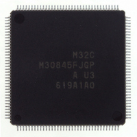
M30845FJGP#U3 Renesas Electronics America, M30845FJGP#U3 Datasheet - Page 286

M30845FJGP#U3
Manufacturer Part Number
M30845FJGP#U3
Description
IC M32C MCU FLASH 512K 144LQFP
Manufacturer
Renesas Electronics America
Series
M16C™ M32C/80r
Specifications of M30845FJGP#U3
Core Processor
M32C/80
Core Size
16/32-Bit
Speed
32MHz
Connectivity
CAN, I²C, IEBus, SIO, UART/USART
Peripherals
DMA, PWM, WDT
Number Of I /o
121
Program Memory Size
512KB (512K x 8)
Program Memory Type
FLASH
Ram Size
24K x 8
Voltage - Supply (vcc/vdd)
3 V ~ 5.5 V
Data Converters
A/D 34x10b, D/A 2x8b
Oscillator Type
Internal
Operating Temperature
-40°C ~ 85°C
Package / Case
144-LQFP
Lead Free Status / RoHS Status
Lead free / RoHS Compliant
Eeprom Size
-
Available stocks
Company
Part Number
Manufacturer
Quantity
Price
- Current page: 286 of 531
- Download datasheet (4Mb)
M
R
R
e
E
3
. v
J
2
0
C
1
18.2.7 Power Consumption Reducing Function
18.2.8 Output Impedance of Sensor Equivalent Circuit under A/D Conversion
9
8 /
0 .
B
When the A/D converter is not used, the VCUT bit in the AD0CON1 register isolates the resistor ladder of
the A/D converter from the reference voltage input pin (V
off any current flow into the resistor ladder from the V
When using the A/D converter, set the VCUT bit to "1" (V
the AD0CON0 register to "1" (A/D conversion started). Do not set the ADST bit and VCUT bit to "1"
simultaneously, nor set the VCUT bit to "0" (no V
bit does not affect the V
For perfect A/D converter performance, complete internal capacitor (C) charging, shown in Figure 18.8,
for the specified period (T) as sampling time. Output Impedance of the sensor equivalent circuit (R
determined by the following equations:
where:
Figure 18.8 shows analog input pin and external sensor equivalent circuit. The impedance (R
obtained if the voltage between pins (V
difference between V
(0.1/1024) means that A/D precision drop, due to insufficient capacitor charge, is held to 0.1LSB at time of A/
D conversion in the 10-bit mode. Actual error, however, is the value of absolute precision added to 0.1LSB.
When ØAD = 10 MHz, T = 0.3 s in the A/D conversion mode with the sample and hold function. Output
impedance (R
Thus, the allowable output impedance of the sensor equivalent circuit, making the precision (error)
0.1LSB or less, is approximately 13.9 k
0
1
4
0
G
3
J
6
u
o r
0 -
. l
V
R = Internal resistance of the microcomputer
X = Precision (error) of the A/D converter
Y = Resolution of the A/D converter (1024 in 10-bit mode, and 256 in 8-bit mode)
Using T = 0.3 s, R = 7.8 k , C = 1.5 pF, X = 0.1, Y = 1024,
R0 = –
u
0
1
p
C
, 7
0
1
(
= Voltage between pins
2
M
When t = T, V
0
3
0
0
2
5
) for sufficiently charging capacitor (C) in the time (T) is determined by the following equation:
C
1.5 X 10
8 /
Page 263
, 4
M
IN
e
–
0.3 X 10
3
–
REF
and V
–12
2
C (R
V
C
R0 = –
C (R0 + R)
C
C
• ln
8 /
f o
performance of the D/A converter.
= V
= V
1
4
0
4
1
C
) T
-6
9
+R)
becomes 0.1LSB.
5
IN
IN
1024
0.1
–
{1 – e
C • ln
T
T= ln
Y
=
X
C
T
) changes from 0 to V
–
–7.8 X10
V
Y
X
maximum.
IN
Y
X
Y
C (R0 + R)
X
= V
1
– R
REF
IN
3
(1 –
= 13.9 X 10
connection) during the A/D conversion. The VCUT
t
REF
}
REF
Y
X
REF
pin.
). Power consumption is reduced by shutting
)
connection) before setting the ADST bit in
IN
-(0.1/1024) V
3
IN
in the time (T), when the
18. A/D Converter
0
) can be
0
) is
Related parts for M30845FJGP#U3
Image
Part Number
Description
Manufacturer
Datasheet
Request
R

Part Number:
Description:
KIT STARTER FOR M16C/29
Manufacturer:
Renesas Electronics America
Datasheet:

Part Number:
Description:
KIT STARTER FOR R8C/2D
Manufacturer:
Renesas Electronics America
Datasheet:

Part Number:
Description:
R0K33062P STARTER KIT
Manufacturer:
Renesas Electronics America
Datasheet:

Part Number:
Description:
KIT STARTER FOR R8C/23 E8A
Manufacturer:
Renesas Electronics America
Datasheet:

Part Number:
Description:
KIT STARTER FOR R8C/25
Manufacturer:
Renesas Electronics America
Datasheet:

Part Number:
Description:
KIT STARTER H8S2456 SHARPE DSPLY
Manufacturer:
Renesas Electronics America
Datasheet:

Part Number:
Description:
KIT STARTER FOR R8C38C
Manufacturer:
Renesas Electronics America
Datasheet:

Part Number:
Description:
KIT STARTER FOR R8C35C
Manufacturer:
Renesas Electronics America
Datasheet:

Part Number:
Description:
KIT STARTER FOR R8CL3AC+LCD APPS
Manufacturer:
Renesas Electronics America
Datasheet:

Part Number:
Description:
KIT STARTER FOR RX610
Manufacturer:
Renesas Electronics America
Datasheet:

Part Number:
Description:
KIT STARTER FOR R32C/118
Manufacturer:
Renesas Electronics America
Datasheet:

Part Number:
Description:
KIT DEV RSK-R8C/26-29
Manufacturer:
Renesas Electronics America
Datasheet:

Part Number:
Description:
KIT STARTER FOR SH7124
Manufacturer:
Renesas Electronics America
Datasheet:

Part Number:
Description:
KIT STARTER FOR H8SX/1622
Manufacturer:
Renesas Electronics America
Datasheet:

Part Number:
Description:
KIT DEV FOR SH7203
Manufacturer:
Renesas Electronics America
Datasheet:


