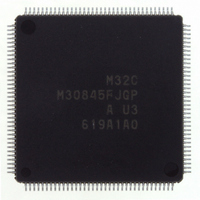
M30845FJGP#U3 Renesas Electronics America, M30845FJGP#U3 Datasheet - Page 252

M30845FJGP#U3
Manufacturer Part Number
M30845FJGP#U3
Description
IC M32C MCU FLASH 512K 144LQFP
Manufacturer
Renesas Electronics America
Series
M16C™ M32C/80r
Specifications of M30845FJGP#U3
Core Processor
M32C/80
Core Size
16/32-Bit
Speed
32MHz
Connectivity
CAN, I²C, IEBus, SIO, UART/USART
Peripherals
DMA, PWM, WDT
Number Of I /o
121
Program Memory Size
512KB (512K x 8)
Program Memory Type
FLASH
Ram Size
24K x 8
Voltage - Supply (vcc/vdd)
3 V ~ 5.5 V
Data Converters
A/D 34x10b, D/A 2x8b
Oscillator Type
Internal
Operating Temperature
-40°C ~ 85°C
Package / Case
144-LQFP
Lead Free Status / RoHS Status
Lead free / RoHS Compliant
Eeprom Size
-
Available stocks
Company
Part Number
Manufacturer
Quantity
Price
- Current page: 252 of 531
- Download datasheet (4Mb)
R
R
M
e
E
3
. v
J
Figure 17.23 Serial Bus Communication Control with SS Pin
2
0
C
17.4.1 SSi Input Pin Function (i=0 to 4)
1
9
0 .
8 /
B
When the SSE bit in the UiSMR3 register is set to "1" (SS function enabled), the special mode 2 is
selected, activating the pin function.
The DINC bit in the UiSMR3 register determines which microcomputer performs as master or slave.
When multiple microcomputers perform as the masters (multi-master system), the SSi pin setting deter-
mines which master microcomputer is active and when.
0
1
17.4.1.1 When Setting the DINC Bit to "1" (Slave Mode)
17.4.1.2 When Setting the DINC Bit to "0" (Master Mode)
4
0
When a high-level ("H") signal is applied to the SSi pin, the STxDi and SRxDi pins are placed in a high-
impedance state and the transfer clock applied to the CLKi pin is ignored. When a low-level ("L") signal
is applied to the SSi input pin, the transfer clock input is valid and serial communication is enabled.
When using the SSi pin functin in master mode, set the UiIRS bit in the UiC1 register to "1" (transmis-
sion completed).
When an "H" signal is applied to the SSi pin, serial communication is available due to transmission
privilege. The master provides the transfer clock output. When an "L" signal is applied to the SSi pin,
it indicates that another master is active. The TxDi and CLKi pins are placed in high-impedance states
and the ERR bit in the UiSMR3 register is set to "1" (fault error) Use the transmit complete interrupt
routine to verify the ERR bit state.
To resume the serial communication after the fault error occurs, set the ERR bit to "0" while applying
the "H" signal to the SSi pin. The TxDi and CLKi pins become ready for signal outputs.
3
G
J
6
u
o r
0 -
. l
______
u
0
1
, 7
0
p
1
(
2
M
0
0
3
5
2
C
8 /
Page 229
, 4
______
_____
M
3
______
2
C
f o
8 /
Microcomputer
4
4
Master
) T
9
P9
P9
P9
5
P9
1(
0(
2(
3(
RxD
CLK
TxD
SS
P1
P1
3
3
3
3
3
2
)
)
)
)
_____
_____
____
____
P9
P9
P9
P9
P9
P9
P9
P9
3(
0(
2(
3(
0(
2(
Microcomputer
1(
1(
Microcomputer
SS
CLK
SRxD
SS
CLK
SRxD
STxD
STxD
3
3
Slave
Slave
)
)
3
3
)
)
3
3
3
3
)
)
)
)
17. Serial I/O (Special Function)
______
_____
Related parts for M30845FJGP#U3
Image
Part Number
Description
Manufacturer
Datasheet
Request
R

Part Number:
Description:
KIT STARTER FOR M16C/29
Manufacturer:
Renesas Electronics America
Datasheet:

Part Number:
Description:
KIT STARTER FOR R8C/2D
Manufacturer:
Renesas Electronics America
Datasheet:

Part Number:
Description:
R0K33062P STARTER KIT
Manufacturer:
Renesas Electronics America
Datasheet:

Part Number:
Description:
KIT STARTER FOR R8C/23 E8A
Manufacturer:
Renesas Electronics America
Datasheet:

Part Number:
Description:
KIT STARTER FOR R8C/25
Manufacturer:
Renesas Electronics America
Datasheet:

Part Number:
Description:
KIT STARTER H8S2456 SHARPE DSPLY
Manufacturer:
Renesas Electronics America
Datasheet:

Part Number:
Description:
KIT STARTER FOR R8C38C
Manufacturer:
Renesas Electronics America
Datasheet:

Part Number:
Description:
KIT STARTER FOR R8C35C
Manufacturer:
Renesas Electronics America
Datasheet:

Part Number:
Description:
KIT STARTER FOR R8CL3AC+LCD APPS
Manufacturer:
Renesas Electronics America
Datasheet:

Part Number:
Description:
KIT STARTER FOR RX610
Manufacturer:
Renesas Electronics America
Datasheet:

Part Number:
Description:
KIT STARTER FOR R32C/118
Manufacturer:
Renesas Electronics America
Datasheet:

Part Number:
Description:
KIT DEV RSK-R8C/26-29
Manufacturer:
Renesas Electronics America
Datasheet:

Part Number:
Description:
KIT STARTER FOR SH7124
Manufacturer:
Renesas Electronics America
Datasheet:

Part Number:
Description:
KIT STARTER FOR H8SX/1622
Manufacturer:
Renesas Electronics America
Datasheet:

Part Number:
Description:
KIT DEV FOR SH7203
Manufacturer:
Renesas Electronics America
Datasheet:


