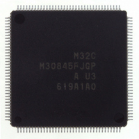
M30845FJGP#U3 Renesas Electronics America, M30845FJGP#U3 Datasheet - Page 182

M30845FJGP#U3
Manufacturer Part Number
M30845FJGP#U3
Description
IC M32C MCU FLASH 512K 144LQFP
Manufacturer
Renesas Electronics America
Series
M16C™ M32C/80r
Specifications of M30845FJGP#U3
Core Processor
M32C/80
Core Size
16/32-Bit
Speed
32MHz
Connectivity
CAN, I²C, IEBus, SIO, UART/USART
Peripherals
DMA, PWM, WDT
Number Of I /o
121
Program Memory Size
512KB (512K x 8)
Program Memory Type
FLASH
Ram Size
24K x 8
Voltage - Supply (vcc/vdd)
3 V ~ 5.5 V
Data Converters
A/D 34x10b, D/A 2x8b
Oscillator Type
Internal
Operating Temperature
-40°C ~ 85°C
Package / Case
144-LQFP
Lead Free Status / RoHS Status
Lead free / RoHS Compliant
Eeprom Size
-
Available stocks
Company
Part Number
Manufacturer
Quantity
Price
- Current page: 182 of 531
- Download datasheet (4Mb)
M
R
R
e
E
3
. v
J
2
Figure 15.6 UDF Register and ONSF Register
0
C
1
9
8 /
0 .
B
0
1
4
0
G
3
J
6
u
o r
0 -
. l
u
One-Shot Start Flag
b7
0
1
Up/Down Flag
b7
NOTES:
p
, 7
0
NOTES:
1
b6
(
1. When read, this bit is set to "0".
2. Overflow or underflow.
b6
2
M
1. Use the MOV instruction to set the UDF register.
2. This bit is enabled when the MR2 bit in the TAiMR register (i=0 to 4) is set to "0" (the UDF register
3. Set this bit to "0" when not using the two-phase pulse signal processing function.
0
b5
3
0
b5
causes increment/decrement switching) in event counter mode.
2
5
C
b4
b4
8 /
Page 159
b3
, 4
b3
b2
M
b2
3
b1
b1
2
(1)
C
b0
b0
8 /
f o
TA0TGH
4
TA0TGL
Symbol
4
TA0OS
TA1OS
TA2OS
TA3OS
TA4OS
TA0UD
TA1UD
TA2UD
TA3UD
TA4UD
TAZIE
Symbol
) T
9
TA2P
TA3P
TA4P
Bit
Bit
5
Symbol
ONSF
Symbol
UDF
Timer A0 One-Shot
Start Flag
Timer A1 One-Shot
Start Flag
Timer A2 One-Shot
Start Flag
Timer A3 One-Shot
Start Flag
Timer A0 Event/Trigger
Select Bit
Timer A4 One-Shot
Start Flag
Z-Phase Input Enable Bit
Timer A0
Up/Down Flag
Timer A1
Up/Down Flag
Timer A2
Up/Down Flag
Timer A3
Up/Down Flag
Timer A4
Up/Down Flag
Timer A2 Two-Phase
Pulse Signal Processing
Function Select Bit
Timer A3 Two-Phase
Pulse Signal Processing
Function Select Bit
Timer A4 Two-Phase
Pulse Signal Processing
Function Select Bit
Bit Name
Bit Name
(1)
(1)
(1)
(1)
(1)
0342
Address
Address
0344
(2)
(2)
(2)
(2)
(2)
16
16
(3)
(3)
(3)
b7b6
0 : In an idle state
1 : Starts the timer
0 : In an idle state
1 : Starts the timer
0 : In an idle state
1 : Starts the timer
0 : In an idle state
1 : Starts the timer
0 : In an idle state
1 : Starts the timer
0 : Disables Z-phase input
1 : Enables Z-phase input
0 0 : Selects an input to the TA0
0 1 : Selects the TB2 overflows
1 0 : Selects the TA4 overflows
1 1 : Selects the TA1 overflows
0 : Decrement
1 : Increment
0 : Decrement
1 : Increment
0 : Decrement
1 : Increment
0 : Decrement
1 : Increment
0 : Decrement
1 : Increment
0 : Disables two-phase pulse signal
1 : Enables two-phase pulse signal
0 : Disables two-phase pulse signal
1 : Enables two-phase pulse signal
0 : Disables two-phase pulse signal
1 : Enables two-phase pulse signal
processing function
processing function
processing function
processing function
processing function
processing function
After Reset
00
16
After Reset
00
16
Function
Function
(2)
(2)
(2)
IN
pin
15. Timer (Timer A)
RW
RW
RW
RW
RW
RW
RW
RW
RW
RW
RW
RW
RW
RW
RW
WO
WO
WO
Related parts for M30845FJGP#U3
Image
Part Number
Description
Manufacturer
Datasheet
Request
R

Part Number:
Description:
KIT STARTER FOR M16C/29
Manufacturer:
Renesas Electronics America
Datasheet:

Part Number:
Description:
KIT STARTER FOR R8C/2D
Manufacturer:
Renesas Electronics America
Datasheet:

Part Number:
Description:
R0K33062P STARTER KIT
Manufacturer:
Renesas Electronics America
Datasheet:

Part Number:
Description:
KIT STARTER FOR R8C/23 E8A
Manufacturer:
Renesas Electronics America
Datasheet:

Part Number:
Description:
KIT STARTER FOR R8C/25
Manufacturer:
Renesas Electronics America
Datasheet:

Part Number:
Description:
KIT STARTER H8S2456 SHARPE DSPLY
Manufacturer:
Renesas Electronics America
Datasheet:

Part Number:
Description:
KIT STARTER FOR R8C38C
Manufacturer:
Renesas Electronics America
Datasheet:

Part Number:
Description:
KIT STARTER FOR R8C35C
Manufacturer:
Renesas Electronics America
Datasheet:

Part Number:
Description:
KIT STARTER FOR R8CL3AC+LCD APPS
Manufacturer:
Renesas Electronics America
Datasheet:

Part Number:
Description:
KIT STARTER FOR RX610
Manufacturer:
Renesas Electronics America
Datasheet:

Part Number:
Description:
KIT STARTER FOR R32C/118
Manufacturer:
Renesas Electronics America
Datasheet:

Part Number:
Description:
KIT DEV RSK-R8C/26-29
Manufacturer:
Renesas Electronics America
Datasheet:

Part Number:
Description:
KIT STARTER FOR SH7124
Manufacturer:
Renesas Electronics America
Datasheet:

Part Number:
Description:
KIT STARTER FOR H8SX/1622
Manufacturer:
Renesas Electronics America
Datasheet:

Part Number:
Description:
KIT DEV FOR SH7203
Manufacturer:
Renesas Electronics America
Datasheet:


