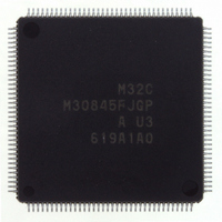
M30845FJGP#U3 Renesas Electronics America, M30845FJGP#U3 Datasheet - Page 509

M30845FJGP#U3
Manufacturer Part Number
M30845FJGP#U3
Description
IC M32C MCU FLASH 512K 144LQFP
Manufacturer
Renesas Electronics America
Series
M16C™ M32C/80r
Specifications of M30845FJGP#U3
Core Processor
M32C/80
Core Size
16/32-Bit
Speed
32MHz
Connectivity
CAN, I²C, IEBus, SIO, UART/USART
Peripherals
DMA, PWM, WDT
Number Of I /o
121
Program Memory Size
512KB (512K x 8)
Program Memory Type
FLASH
Ram Size
24K x 8
Voltage - Supply (vcc/vdd)
3 V ~ 5.5 V
Data Converters
A/D 34x10b, D/A 2x8b
Oscillator Type
Internal
Operating Temperature
-40°C ~ 85°C
Package / Case
144-LQFP
Lead Free Status / RoHS Status
Lead free / RoHS Compliant
Eeprom Size
-
Available stocks
Company
Part Number
Manufacturer
Quantity
Price
- Current page: 509 of 531
- Download datasheet (4Mb)
M
R
R
e
E
3
. v
J
2
0
C
1
9
8 /
0 .
B
• Wrong values are stored in the AD0i register (i=0 to 7) if the CPU reads the AD0i register while the AD0i
• Conversion results of the A/D converter are indeterminate if the ADST bit in the AD0CON0 register is set
• External triggers cannot be used in DMAC operating mode. Do not read the AD00 register by program.
• Do not perform the A/D conversion in wait mode.
• Set the MCD4 to MCD0 bits in the MCD register to "10010
• Do not acknowledge any interrupt requests, even if generated, before setting the ADST bit, if the A/D
• AV
0
In one-shot mode or single sweep mode, read the corresponding AD0i register after verifying that the A/D
If the ADST bit is changed to "0" by program, during the A/D conversion, do not use any values obtained
1
register stores results from a completed A/D conversion. This occurs when the CPU clock is set to a
divided main clock or a sub clock.
conversion has been completed. The IR bit in the AD0IC register determines the completion of the A/D
conversion.
In repeat mode, repeat sweep mode 0, repeat sweep mode 1, multi-port single sweep mode, and multi-
port repeat sweep mode 0, use an undivided main clock as the CPU clock.
to "0" (stop A/D conversion) and the conversion is forcibly terminated by program during the A/D conver-
sion. The AD0i register not performing the A/D conversion may also be indeterminate.
from the AD0i registers.
function.
conversion is terminated by setting the ADST bit in the AD0CON0 register to "0" (A/D conversion
stopped) while the microcomputer is A/D converting in single sweep mode.
4
0
A/D input voltage (for AN
A/D input voltage (for AN0
G
3
J
6
u
o r
CC
0 -
. l
u
0
1
p
, 7
= V
0
1
(
2
M
0
REF
3
0
2
5
C
= V
8 /
Page 486
, 4
CC1
M
3
2
V
C
CC2
0
8 /
f o
0
to AN
4
4
to AN0
) T
,
9
5
7
, AN15
7
, and AN2
0
to AN15
0
to AN2
7
, ANEX0, and ANEX1)
7
)
2
" (no division) if using the sample and hold
V
CC2
.
27. Precautions (A/D Converter)
V
CC1
,
Related parts for M30845FJGP#U3
Image
Part Number
Description
Manufacturer
Datasheet
Request
R

Part Number:
Description:
KIT STARTER FOR M16C/29
Manufacturer:
Renesas Electronics America
Datasheet:

Part Number:
Description:
KIT STARTER FOR R8C/2D
Manufacturer:
Renesas Electronics America
Datasheet:

Part Number:
Description:
R0K33062P STARTER KIT
Manufacturer:
Renesas Electronics America
Datasheet:

Part Number:
Description:
KIT STARTER FOR R8C/23 E8A
Manufacturer:
Renesas Electronics America
Datasheet:

Part Number:
Description:
KIT STARTER FOR R8C/25
Manufacturer:
Renesas Electronics America
Datasheet:

Part Number:
Description:
KIT STARTER H8S2456 SHARPE DSPLY
Manufacturer:
Renesas Electronics America
Datasheet:

Part Number:
Description:
KIT STARTER FOR R8C38C
Manufacturer:
Renesas Electronics America
Datasheet:

Part Number:
Description:
KIT STARTER FOR R8C35C
Manufacturer:
Renesas Electronics America
Datasheet:

Part Number:
Description:
KIT STARTER FOR R8CL3AC+LCD APPS
Manufacturer:
Renesas Electronics America
Datasheet:

Part Number:
Description:
KIT STARTER FOR RX610
Manufacturer:
Renesas Electronics America
Datasheet:

Part Number:
Description:
KIT STARTER FOR R32C/118
Manufacturer:
Renesas Electronics America
Datasheet:

Part Number:
Description:
KIT DEV RSK-R8C/26-29
Manufacturer:
Renesas Electronics America
Datasheet:

Part Number:
Description:
KIT STARTER FOR SH7124
Manufacturer:
Renesas Electronics America
Datasheet:

Part Number:
Description:
KIT STARTER FOR H8SX/1622
Manufacturer:
Renesas Electronics America
Datasheet:

Part Number:
Description:
KIT DEV FOR SH7203
Manufacturer:
Renesas Electronics America
Datasheet:


