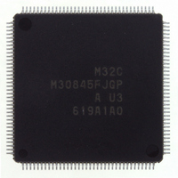
M30845FJGP#U3 Renesas Electronics America, M30845FJGP#U3 Datasheet - Page 420

M30845FJGP#U3
Manufacturer Part Number
M30845FJGP#U3
Description
IC M32C MCU FLASH 512K 144LQFP
Manufacturer
Renesas Electronics America
Series
M16C™ M32C/80r
Specifications of M30845FJGP#U3
Core Processor
M32C/80
Core Size
16/32-Bit
Speed
32MHz
Connectivity
CAN, I²C, IEBus, SIO, UART/USART
Peripherals
DMA, PWM, WDT
Number Of I /o
121
Program Memory Size
512KB (512K x 8)
Program Memory Type
FLASH
Ram Size
24K x 8
Voltage - Supply (vcc/vdd)
3 V ~ 5.5 V
Data Converters
A/D 34x10b, D/A 2x8b
Oscillator Type
Internal
Operating Temperature
-40°C ~ 85°C
Package / Case
144-LQFP
Lead Free Status / RoHS Status
Lead free / RoHS Compliant
Eeprom Size
-
Available stocks
Company
Part Number
Manufacturer
Quantity
Price
- Current page: 420 of 531
- Download datasheet (4Mb)
R
R
M
25.1 Memory Map
e
E
3
. v
J
2
Figure 25.1 Flash Memory Block Diagram
0
C
The flash memory includes the user ROM area and the boot ROM area. The user ROM area has space to
store the microcomputer operating programs in single-chip mode or memory expansion mode, and a sepa-
rate 4-kbyte space as the block A. Figure 25.1 shows a block diagram of the flash memory.
The user ROM area is divided into several blocks, each of which can be protected (locked) from program or
erase. The user ROM area can be rewritten in CPU rewrite mode, standard serial I/O mode and parallel I/O
mode.
The boot ROM area is located at the same addresses as the user ROM area. It can only be rewritten in
parallel I/O mode. A program in the boot ROM area is executed after a hardware reset occurs while a high-
level ("H") signal is applied to the CNV
A program in the user ROM area is executed after a hardware reset occurs while an "L" signal is applied to
the CNV
1
9
0 .
B
8 /
0
1
4
0
00F000
00FFFF
F80000
F8FFFF
F90000
F9FFFF
FA0000
FAFFFF
FB0000
FBFFFF
FC0000
FCFFFF
FD0000
FDFFFF
FE0000
FEFFFF
FF0000
FFFFFF
NOTES:
3
J
G
6
u
o r
0 -
. l
1. The boot ROM area can be rewritten in parallel I/O mode only.
2. When specifying a block, use an even address in the block to be specified.
3. Shown here is a flash memory block diagram in single-chip mode.
4. The block A cannot be erased by the all erase unlocked block command. Use the block erase command to erase.
SS
u
0
1
16
16
16
16
16
16
16
16
16
16
16
16
16
16
16
16
16
16
, 7
0
p
1
pin. Consequently, the boot ROM area cannot be read.
(
2
Block 0 to Block 5 (32+8+8+8
M
0
0
3
Block 12 : 64 Kbytes
Block 11 : 64 Kbytes
Block 10 : 64 Kbytes
Block 6 : 64 Kbytes
Block 9 : 64 Kbytes
Block 8 : 64 Kbytes
Block 7 : 64 Kbytes
5
2
Block A :4 Kbytes
C
+4+4) Kbytes
8 /
Page 397
, 4
M
3
2
(4)
C
f o
8 /
User ROM area
4
4
) T
9
5
SS
and P5
FF0000
FF7FFF
FF8000
FF9FFF
FFA000
FFBFFF
FFC000
FFDFFF
FFE000
FFEFFF
FFF000
FFFFFF
16
16
16
16
16
16
16
16
16
16
16
16
0
pins and a low-level ("L") signal is applied to the P5
Block 5 : 32 Kbytes
Block 4 : 8 Kbytes
Block 3 : 8 Kbytes
Block 2 : 8 Kbytes
Block 1 : 4 Kbytes
Block 0 : 4 Kbytes
FFF000
FFFFFF
16
16
25. Flash Memory Version
Boot ROM area
4 Kbytes
(1)
5
pin.
Related parts for M30845FJGP#U3
Image
Part Number
Description
Manufacturer
Datasheet
Request
R

Part Number:
Description:
KIT STARTER FOR M16C/29
Manufacturer:
Renesas Electronics America
Datasheet:

Part Number:
Description:
KIT STARTER FOR R8C/2D
Manufacturer:
Renesas Electronics America
Datasheet:

Part Number:
Description:
R0K33062P STARTER KIT
Manufacturer:
Renesas Electronics America
Datasheet:

Part Number:
Description:
KIT STARTER FOR R8C/23 E8A
Manufacturer:
Renesas Electronics America
Datasheet:

Part Number:
Description:
KIT STARTER FOR R8C/25
Manufacturer:
Renesas Electronics America
Datasheet:

Part Number:
Description:
KIT STARTER H8S2456 SHARPE DSPLY
Manufacturer:
Renesas Electronics America
Datasheet:

Part Number:
Description:
KIT STARTER FOR R8C38C
Manufacturer:
Renesas Electronics America
Datasheet:

Part Number:
Description:
KIT STARTER FOR R8C35C
Manufacturer:
Renesas Electronics America
Datasheet:

Part Number:
Description:
KIT STARTER FOR R8CL3AC+LCD APPS
Manufacturer:
Renesas Electronics America
Datasheet:

Part Number:
Description:
KIT STARTER FOR RX610
Manufacturer:
Renesas Electronics America
Datasheet:

Part Number:
Description:
KIT STARTER FOR R32C/118
Manufacturer:
Renesas Electronics America
Datasheet:

Part Number:
Description:
KIT DEV RSK-R8C/26-29
Manufacturer:
Renesas Electronics America
Datasheet:

Part Number:
Description:
KIT STARTER FOR SH7124
Manufacturer:
Renesas Electronics America
Datasheet:

Part Number:
Description:
KIT STARTER FOR H8SX/1622
Manufacturer:
Renesas Electronics America
Datasheet:

Part Number:
Description:
KIT DEV FOR SH7203
Manufacturer:
Renesas Electronics America
Datasheet:


