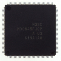
M30845FJGP#U3 Renesas Electronics America, M30845FJGP#U3 Datasheet - Page 276

M30845FJGP#U3
Manufacturer Part Number
M30845FJGP#U3
Description
IC M32C MCU FLASH 512K 144LQFP
Manufacturer
Renesas Electronics America
Series
M16C™ M32C/80r
Specifications of M30845FJGP#U3
Core Processor
M32C/80
Core Size
16/32-Bit
Speed
32MHz
Connectivity
CAN, I²C, IEBus, SIO, UART/USART
Peripherals
DMA, PWM, WDT
Number Of I /o
121
Program Memory Size
512KB (512K x 8)
Program Memory Type
FLASH
Ram Size
24K x 8
Voltage - Supply (vcc/vdd)
3 V ~ 5.5 V
Data Converters
A/D 34x10b, D/A 2x8b
Oscillator Type
Internal
Operating Temperature
-40°C ~ 85°C
Package / Case
144-LQFP
Lead Free Status / RoHS Status
Lead free / RoHS Compliant
Eeprom Size
-
Available stocks
Company
Part Number
Manufacturer
Quantity
Price
- Current page: 276 of 531
- Download datasheet (4Mb)
M
R
R
e
E
3
. v
J
2
Figure 18.6 AD0CON4 Register and AD00 to AD07 Registers
0
C
1
9
8 /
0 .
B
0
1
4
0
b15
G
3
J
A/D0 Register i (i =0 to 7)
6
u
NOTES:
o r
0 -
. l
A/D0 Control Register 4
b7
0 0 0 0
1. In DMAC operating mode, register value read by program is indeterminate.
2. Register value is indeterminate when written while the A/D conversion is stopped.
3. Register value is indeterminate if the next A/D conversion result is stored before reading the register.
4. The AD00 register is available in DMAC operating mode. Other registers are indeterminate.
5. In DMAC operating mode and 10-bit mode, set DMAC for a 16-bit transfer.
u
NOTES:
0
1
p
, 7
0
4. When the MSS bit in the AD0CON3 regsiter is set to "0" (multi-port sweep mode disabled), set the
b6
1. When the AD0CON4 register is rewritten during the A/D conversion, the conversion result is
2. The MPS11 and MPS10 bits cannot be set to "01
3. The MPS11 and MPS10 bits can be set to "10
1
(
2
M
indeterminate.
MPS11 and MPS10 bits to "00
When the MSS bit is set to "1" (multi-port sweep mode enabled), set the MPS11 and MPS10 bits to
"01
0
b5
3
0
b8
2
2
5
", "10
b7
b4
C
8 /
Page 253
b3
, 4
2
" or "11
b2
M
3
b1
0 0
2
b0
2
C
".
b0
Symbol
AD00
AD01 to AD03 0383
AD04 to AD06 0389
AD07
8 low-order bits in an A/D conversion result
In 10-bit mode
In 8-bit mode
8 /
f o
When read, its content is indeterminate.
4
(b1 - b0)
(b7 - b4)
4
Symbol
MPS10
MPS11
) T
9
Bit
5
Symbol
AD0CON4
2
(1, 2, 3, 4, 5)
(1)
".
Multi-Port Sweep
Port Select Bit
Reserved Bit
Reserved Bit
Address
0381
038F
16
16
16
16
Bit Name
: 2 high-order bits in an A/D conversion result
: When read, its content is indeterminate.
- 0380
- 0382
- 0388
- 038E
2
16
16
16
" or "11
16
(2, 3)
, 0385
, 038B
2
" in the 100-pin package.
Address
0392
2
Function
16
16
16
" in single-chip mode only.
Set to "0".
When read, its content is indeterminate.
Set to "0".
When read, its content is indeterminate.
b3 b2
0 0 : (Note 4)
0 1 : AN
1 0 : AN
1 1 : AN
- 0384
- 038A
16
16
, 0387
, 038D
0
0
0
to AN
to AN
to AN
16
16
Function
After Reset
XXXX 00XX
7
7
7
- 0386
, AN15
, AN0
, AN2
- 038C
16
0
0
16
0
to AN0
to AN2
to AN15
After Reset
00000000 XXXXXXXX
Indeterminate
Indeterminate
Indeterminate
2
7
7
7
18. A/D Converter
RW
RO
RO
RO
RW
RW
RW
RW
RW
2
Related parts for M30845FJGP#U3
Image
Part Number
Description
Manufacturer
Datasheet
Request
R

Part Number:
Description:
KIT STARTER FOR M16C/29
Manufacturer:
Renesas Electronics America
Datasheet:

Part Number:
Description:
KIT STARTER FOR R8C/2D
Manufacturer:
Renesas Electronics America
Datasheet:

Part Number:
Description:
R0K33062P STARTER KIT
Manufacturer:
Renesas Electronics America
Datasheet:

Part Number:
Description:
KIT STARTER FOR R8C/23 E8A
Manufacturer:
Renesas Electronics America
Datasheet:

Part Number:
Description:
KIT STARTER FOR R8C/25
Manufacturer:
Renesas Electronics America
Datasheet:

Part Number:
Description:
KIT STARTER H8S2456 SHARPE DSPLY
Manufacturer:
Renesas Electronics America
Datasheet:

Part Number:
Description:
KIT STARTER FOR R8C38C
Manufacturer:
Renesas Electronics America
Datasheet:

Part Number:
Description:
KIT STARTER FOR R8C35C
Manufacturer:
Renesas Electronics America
Datasheet:

Part Number:
Description:
KIT STARTER FOR R8CL3AC+LCD APPS
Manufacturer:
Renesas Electronics America
Datasheet:

Part Number:
Description:
KIT STARTER FOR RX610
Manufacturer:
Renesas Electronics America
Datasheet:

Part Number:
Description:
KIT STARTER FOR R32C/118
Manufacturer:
Renesas Electronics America
Datasheet:

Part Number:
Description:
KIT DEV RSK-R8C/26-29
Manufacturer:
Renesas Electronics America
Datasheet:

Part Number:
Description:
KIT STARTER FOR SH7124
Manufacturer:
Renesas Electronics America
Datasheet:

Part Number:
Description:
KIT STARTER FOR H8SX/1622
Manufacturer:
Renesas Electronics America
Datasheet:

Part Number:
Description:
KIT DEV FOR SH7203
Manufacturer:
Renesas Electronics America
Datasheet:


