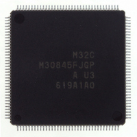
M30845FJGP#U3 Renesas Electronics America, M30845FJGP#U3 Datasheet - Page 331

M30845FJGP#U3
Manufacturer Part Number
M30845FJGP#U3
Description
IC M32C MCU FLASH 512K 144LQFP
Manufacturer
Renesas Electronics America
Series
M16C™ M32C/80r
Specifications of M30845FJGP#U3
Core Processor
M32C/80
Core Size
16/32-Bit
Speed
32MHz
Connectivity
CAN, I²C, IEBus, SIO, UART/USART
Peripherals
DMA, PWM, WDT
Number Of I /o
121
Program Memory Size
512KB (512K x 8)
Program Memory Type
FLASH
Ram Size
24K x 8
Voltage - Supply (vcc/vdd)
3 V ~ 5.5 V
Data Converters
A/D 34x10b, D/A 2x8b
Oscillator Type
Internal
Operating Temperature
-40°C ~ 85°C
Package / Case
144-LQFP
Lead Free Status / RoHS Status
Lead free / RoHS Compliant
Eeprom Size
-
Available stocks
Company
Part Number
Manufacturer
Quantity
Price
- Current page: 331 of 531
- Download datasheet (4Mb)
R
R
M
e
E
3
. v
J
2
Figure 22.28 G0CMP0 to G0CMP3 Registers and G1CMP0 to G1CMP3 Registers
9 0
C
. 1
8 /
B
1 0
0
4
3 0
G
J
- 6
. l u
o r
b15
Receive CRC Code Register i
Data Compare Register ij
Data Mask Register ij
Transmit CRC Code Register i
b7
b7
b15
1 0
u
NOTES:
NOTES:
0
NOTES:
p
, 7
1 0
1. The calculated result is reset by setting the RCRCE bit in the GiERC register to "0" (not used).
2. The result is reset to the default value selected by the CRCV bit in the GiEMR register before
3. Receive CRC calculation is performed with every bit of data received while the RCRCE bit in the
1. The calculated result is reset by setting the TE bit in the GiCR register to "0" (transmit disabled).
(
2. Transmit CRC calculation is performed with each bit of data transmitted while the TCRCE bit in
1. Set the GiMSK0 register to use the GiCMP0 register.
0 2
M
G0MSK0 and G0MSK1 Registers, G1MSK0 and G1MSK1 Registers
G0TCRC and G1TCRC Registers, G0RCRC and G1RCRC Registers
If the ACRC bit in the GiEMR register is set to "1" (reset), the result is reset by matching data in the
GiCMPj register (j=0 to 3) with the received data.
reception starts.
GiERC register is set to "1" (used).
The CRCV bit in the GiEMR register selects a default value.
the GiETC register is set to "1" (used).
Set the GiMSK1 register to use the GiCMP1 register.
5 0
3
2
b8
b8
C
8 /
b7
b7
Page 308
, 4
M
3
2
C
b0
b0
b0
b0
f o
8 /
4
4
Masked data for received data
Set incomparable bit to "1"
Result of the transmit CRC calculation
) T
5 9
Result of the receive CRC calculation
Data to be compared
Symbol
G0CMP0 to G0CMP3
G1CMP0 to G1CMP3
Symbol
G0MSK0, G0MSK1
G1MSK0, G1MSK1
Symbol
G0TCRC, G1TCRC
Symbol
G0RCRC, G1RCRC
(i=0,1, j=0,1)
(i=0,1, j=0 to 3)
(i=0,1)
(i=0,1)
Function
Function
Address
00F9
Address
00F0
0130
Function
Address
00F4
0134
Address
00FB
16-
16
16
00F8
, 0131
, 00F1
16
16
16
Function
, 0135
, 00F5
-00FA
(1, 2)
16
(1, 2, 3)
22. Intelligent I/O (Communication Function)
16
, 0139
16
, 0132
, 00F2
16
16
16
, 013B
16
16
-0138
16
, 0133
, 00F3
16
-013A
16
Setting Range
Setting Range
16
00
00
16
16 to
16 to
16
After Reset
Indeterminate
Indeterminate
After Reset
Indeterminate
After Reset
Indeterminate
Indeterminate
FF
FF
16
16
After Reset
0000
16
RW
RW
RW
RW
RW
RW
RO
RO
Related parts for M30845FJGP#U3
Image
Part Number
Description
Manufacturer
Datasheet
Request
R

Part Number:
Description:
KIT STARTER FOR M16C/29
Manufacturer:
Renesas Electronics America
Datasheet:

Part Number:
Description:
KIT STARTER FOR R8C/2D
Manufacturer:
Renesas Electronics America
Datasheet:

Part Number:
Description:
R0K33062P STARTER KIT
Manufacturer:
Renesas Electronics America
Datasheet:

Part Number:
Description:
KIT STARTER FOR R8C/23 E8A
Manufacturer:
Renesas Electronics America
Datasheet:

Part Number:
Description:
KIT STARTER FOR R8C/25
Manufacturer:
Renesas Electronics America
Datasheet:

Part Number:
Description:
KIT STARTER H8S2456 SHARPE DSPLY
Manufacturer:
Renesas Electronics America
Datasheet:

Part Number:
Description:
KIT STARTER FOR R8C38C
Manufacturer:
Renesas Electronics America
Datasheet:

Part Number:
Description:
KIT STARTER FOR R8C35C
Manufacturer:
Renesas Electronics America
Datasheet:

Part Number:
Description:
KIT STARTER FOR R8CL3AC+LCD APPS
Manufacturer:
Renesas Electronics America
Datasheet:

Part Number:
Description:
KIT STARTER FOR RX610
Manufacturer:
Renesas Electronics America
Datasheet:

Part Number:
Description:
KIT STARTER FOR R32C/118
Manufacturer:
Renesas Electronics America
Datasheet:

Part Number:
Description:
KIT DEV RSK-R8C/26-29
Manufacturer:
Renesas Electronics America
Datasheet:

Part Number:
Description:
KIT STARTER FOR SH7124
Manufacturer:
Renesas Electronics America
Datasheet:

Part Number:
Description:
KIT STARTER FOR H8SX/1622
Manufacturer:
Renesas Electronics America
Datasheet:

Part Number:
Description:
KIT DEV FOR SH7203
Manufacturer:
Renesas Electronics America
Datasheet:


