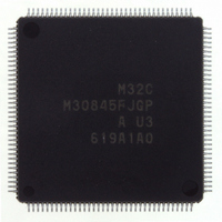
M30845FJGP#U3 Renesas Electronics America, M30845FJGP#U3 Datasheet - Page 205

M30845FJGP#U3
Manufacturer Part Number
M30845FJGP#U3
Description
IC M32C MCU FLASH 512K 144LQFP
Manufacturer
Renesas Electronics America
Series
M16C™ M32C/80r
Specifications of M30845FJGP#U3
Core Processor
M32C/80
Core Size
16/32-Bit
Speed
32MHz
Connectivity
CAN, I²C, IEBus, SIO, UART/USART
Peripherals
DMA, PWM, WDT
Number Of I /o
121
Program Memory Size
512KB (512K x 8)
Program Memory Type
FLASH
Ram Size
24K x 8
Voltage - Supply (vcc/vdd)
3 V ~ 5.5 V
Data Converters
A/D 34x10b, D/A 2x8b
Oscillator Type
Internal
Operating Temperature
-40°C ~ 85°C
Package / Case
144-LQFP
Lead Free Status / RoHS Status
Lead free / RoHS Compliant
Eeprom Size
-
Available stocks
Company
Part Number
Manufacturer
Quantity
Price
- Current page: 205 of 531
- Download datasheet (4Mb)
R
R
M
16. Three-Phase Motor Control Timer Functions
e
E
3
. v
J
Table 16.1 Three-Phase Motor Control Timer Functions Specification
2
NOTES:
0
Three-Phase Waveform Output Pin
Forced Cutoff
Timers to be Used
Output Waveform
Carrier Wave Cycle
Three-Phase PWM Output Width
Dead Time
Active Level
Positive- and Negative-Phase Con- Positive and negative-phases concurrent active disable function
current Active Disable Function
Interrupt Frequency
Three-phase motor driving waveform can be output by using the timers A1, A2, A4 and B2. Table 16.1 lists
specifications of the three-phase motor control timer functions. Table 16.2 lists pin settings. Figure 16.1
shows a block diagram. Figures 16.2 to 16.7 show registers associated with the three-phase motor control
timer functions.
C
1
9
0 .
B
8 /
1. Forced cutoff by the signal applied to the NMI pin is available when the INV02 bit is set to "1" (three-
2. The CNT3 to CNT0 bits in the TCSPR register select no division (n=0) or divide-by-2n (n=1 to 15).
0
1
4
0
phase motor control timer functions) and the INV03 bit is set to "1" (three-phase motor control timer
output enabled).
3
J
G
6
u
o r
0 -
. l
0
1
u
, 7
0
p
1
(1)
(
2
Item
M
0
0
3
5
2
C
8 /
Page 182
, 4
M
3
2
C
f o
8 /
4
4
9
) T
Six pins (U, U, V, V, W, W)
Apply a low-level ("L") signal to the NMI pin
Timer A4, A1, A2 (used in one-shot timer mode):
Timer B2 (used in timer mode):
Dead time timer (three 8-bit timers share reload register):
Triangular wave modulation, Sawtooth wave modulation
Triangular wave modulation:
Sawtooth wave modulation:
Triangular wave modulation:
Sawtooth wave modulation:
Count source
Selected from a high level ("H") or low level ("L")
Positive and negative-phases concurrent active detect function
For the timer B2 interrupt, one carrier wave cycle-to-cycle basis through 15
time- carrier wave cycle-to-cycle basis can be selected
5
Timer A4: U- and U-phase waveform control
Timer A1: V- and V-phase waveform control
Timer A2: W- and W-phase waveform control
Carrier wave cycle control
Dead time control
Can output a high-level waveform or a low-level waveform for one cycle;
Can set positive-phase level and negative-phase level separately
m
Count source: f
n
TA2 and TA21 registers when setting the INV11 bit to "1"), 0001
Count source: f
p
Count source: f
: setting value of the DTT register, 01
: setting value of the TA4, TA1 and TA2 register (of the TA4, TA41, TA1, TA11,
: setting value of the TB2 register, 0000
___
_______
x
p
, or no dead time
1
1
1
___
, f
, f
, or f
___
___
8
8
___
, f
, f
1
2n
2n
___
divided by 2
(2)
(2)
, f
, f
count source
count source
16. Three-Phase Motor Control Timer Functions
c32
c32
count source
count source
Specification
_______
16
x
x
x
x
to FF
16
(m+1)
n
(m+1)
n
to FFFF
x
2
16
x
2
16
16
to FFFF
16
Related parts for M30845FJGP#U3
Image
Part Number
Description
Manufacturer
Datasheet
Request
R

Part Number:
Description:
KIT STARTER FOR M16C/29
Manufacturer:
Renesas Electronics America
Datasheet:

Part Number:
Description:
KIT STARTER FOR R8C/2D
Manufacturer:
Renesas Electronics America
Datasheet:

Part Number:
Description:
R0K33062P STARTER KIT
Manufacturer:
Renesas Electronics America
Datasheet:

Part Number:
Description:
KIT STARTER FOR R8C/23 E8A
Manufacturer:
Renesas Electronics America
Datasheet:

Part Number:
Description:
KIT STARTER FOR R8C/25
Manufacturer:
Renesas Electronics America
Datasheet:

Part Number:
Description:
KIT STARTER H8S2456 SHARPE DSPLY
Manufacturer:
Renesas Electronics America
Datasheet:

Part Number:
Description:
KIT STARTER FOR R8C38C
Manufacturer:
Renesas Electronics America
Datasheet:

Part Number:
Description:
KIT STARTER FOR R8C35C
Manufacturer:
Renesas Electronics America
Datasheet:

Part Number:
Description:
KIT STARTER FOR R8CL3AC+LCD APPS
Manufacturer:
Renesas Electronics America
Datasheet:

Part Number:
Description:
KIT STARTER FOR RX610
Manufacturer:
Renesas Electronics America
Datasheet:

Part Number:
Description:
KIT STARTER FOR R32C/118
Manufacturer:
Renesas Electronics America
Datasheet:

Part Number:
Description:
KIT DEV RSK-R8C/26-29
Manufacturer:
Renesas Electronics America
Datasheet:

Part Number:
Description:
KIT STARTER FOR SH7124
Manufacturer:
Renesas Electronics America
Datasheet:

Part Number:
Description:
KIT STARTER FOR H8SX/1622
Manufacturer:
Renesas Electronics America
Datasheet:

Part Number:
Description:
KIT DEV FOR SH7203
Manufacturer:
Renesas Electronics America
Datasheet:


