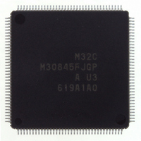
M30845FJGP#U3 Renesas Electronics America, M30845FJGP#U3 Datasheet - Page 386

M30845FJGP#U3
Manufacturer Part Number
M30845FJGP#U3
Description
IC M32C MCU FLASH 512K 144LQFP
Manufacturer
Renesas Electronics America
Series
M16C™ M32C/80r
Specifications of M30845FJGP#U3
Core Processor
M32C/80
Core Size
16/32-Bit
Speed
32MHz
Connectivity
CAN, I²C, IEBus, SIO, UART/USART
Peripherals
DMA, PWM, WDT
Number Of I /o
121
Program Memory Size
512KB (512K x 8)
Program Memory Type
FLASH
Ram Size
24K x 8
Voltage - Supply (vcc/vdd)
3 V ~ 5.5 V
Data Converters
A/D 34x10b, D/A 2x8b
Oscillator Type
Internal
Operating Temperature
-40°C ~ 85°C
Package / Case
144-LQFP
Lead Free Status / RoHS Status
Lead free / RoHS Compliant
Eeprom Size
-
Available stocks
Company
Part Number
Manufacturer
Quantity
Price
- Current page: 386 of 531
- Download datasheet (4Mb)
M
R
R
e
E
3
. v
J
Figure 23.34 C0SLOT0_6 to C0SLOT0_13, C0SLOT1_6 to C0SLOT1_13, C0SLOT0_14,
2
0
C
1
9
8 /
0 .
B
The message slot, selected by setting the C0SBS register, is read by reading the message slot buffer. A
message can be written in the message slot selected by the C0SBS register if the message is written to
the message slot buffer.
Write to the message slot k (k=0 to 15) while the corresponing C0MCTLk register is set to "00
0
1
4
0
G
3
J
6
u
CAN0 Message Slot Buffer j Data m
o r
CAN0 Message Slot Buffer j Time Stamp High-Ordered
CAN0 Message Slot Buffer j Time Stamp Low-Ordered
b7
0 -
. l
b7
b7
u
NOTES:
NOTES:
0
1
p
, 7
0
NOTES:
1
1. Select, by setting the C0SBS register, the time stamp high-ordered in the message slot k to be
1. Select, by setting the C0SBS register, the time stamp low-ordered in the message slot k to be
(
2
M
C0SLOT1_14, C0SLOT0_15 and C0SLOT1_15 Registers
accessed by the C0SLOTj_15 register.
0
1. Select, by setting the C0SBS register, the data m in the message slot k to be accessed by the
2. When the data frame is received, data with less than the data length selected by the C0SLOTj_5
accessed by the C0SLOTj_14 register.
3
0
2
5
C0SLOTj_6 to C0SLOTj_13 registers.
register is indeterminate.
C
8 /
Page 363
, 4
M
3
2
C
b0
b0
b0
8 /
f o
Read or write data m in the message slot k
(k=0 to 15)
Read or write the time stamp high-ordered
in the message slot k (k=0 to 15)
Read or write the time stamp low-ordered
in the message slot k (k=0 to 15)
4
4
) T
9
5
Symbol
C0SLOT0_6 to C0SLOT0_13
C1SLOT0_6 to C1SLOT0_13
Symbol
C0SLOT0_14, C0SLOT1_14
Symbol
C0SLOT0_15, C0SLOT1_15
Function
Function
Function
(j=0,1, m=0 to 7)
01EE
Address
01EF
Address
01E6
01F6
Address
16,
16,
16
16
01FE
- 01ED
- 01FD
01FF
(1, 2)
16
16
16
16
After Reset
Indeterminate
After Reset
Indeterminate
00
Setting Range
Setting Range
16
(j=0,1) (1)
00
00
Setting Range
(j=0,1)
to FF
16
16
to FF
to FF
After Reset
Indeterminate
Indeterminate
16
(1)
16
16
23. CAN Module
RW
RW
RW
RW
RW
RW
16
".
Related parts for M30845FJGP#U3
Image
Part Number
Description
Manufacturer
Datasheet
Request
R

Part Number:
Description:
KIT STARTER FOR M16C/29
Manufacturer:
Renesas Electronics America
Datasheet:

Part Number:
Description:
KIT STARTER FOR R8C/2D
Manufacturer:
Renesas Electronics America
Datasheet:

Part Number:
Description:
R0K33062P STARTER KIT
Manufacturer:
Renesas Electronics America
Datasheet:

Part Number:
Description:
KIT STARTER FOR R8C/23 E8A
Manufacturer:
Renesas Electronics America
Datasheet:

Part Number:
Description:
KIT STARTER FOR R8C/25
Manufacturer:
Renesas Electronics America
Datasheet:

Part Number:
Description:
KIT STARTER H8S2456 SHARPE DSPLY
Manufacturer:
Renesas Electronics America
Datasheet:

Part Number:
Description:
KIT STARTER FOR R8C38C
Manufacturer:
Renesas Electronics America
Datasheet:

Part Number:
Description:
KIT STARTER FOR R8C35C
Manufacturer:
Renesas Electronics America
Datasheet:

Part Number:
Description:
KIT STARTER FOR R8CL3AC+LCD APPS
Manufacturer:
Renesas Electronics America
Datasheet:

Part Number:
Description:
KIT STARTER FOR RX610
Manufacturer:
Renesas Electronics America
Datasheet:

Part Number:
Description:
KIT STARTER FOR R32C/118
Manufacturer:
Renesas Electronics America
Datasheet:

Part Number:
Description:
KIT DEV RSK-R8C/26-29
Manufacturer:
Renesas Electronics America
Datasheet:

Part Number:
Description:
KIT STARTER FOR SH7124
Manufacturer:
Renesas Electronics America
Datasheet:

Part Number:
Description:
KIT STARTER FOR H8SX/1622
Manufacturer:
Renesas Electronics America
Datasheet:

Part Number:
Description:
KIT DEV FOR SH7203
Manufacturer:
Renesas Electronics America
Datasheet:


