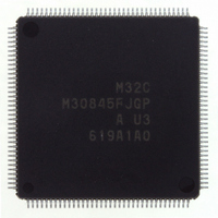
M30845FJGP#U3 Renesas Electronics America, M30845FJGP#U3 Datasheet - Page 66

M30845FJGP#U3
Manufacturer Part Number
M30845FJGP#U3
Description
IC M32C MCU FLASH 512K 144LQFP
Manufacturer
Renesas Electronics America
Series
M16C™ M32C/80r
Specifications of M30845FJGP#U3
Core Processor
M32C/80
Core Size
16/32-Bit
Speed
32MHz
Connectivity
CAN, I²C, IEBus, SIO, UART/USART
Peripherals
DMA, PWM, WDT
Number Of I /o
121
Program Memory Size
512KB (512K x 8)
Program Memory Type
FLASH
Ram Size
24K x 8
Voltage - Supply (vcc/vdd)
3 V ~ 5.5 V
Data Converters
A/D 34x10b, D/A 2x8b
Oscillator Type
Internal
Operating Temperature
-40°C ~ 85°C
Package / Case
144-LQFP
Lead Free Status / RoHS Status
Lead free / RoHS Compliant
Eeprom Size
-
Available stocks
Company
Part Number
Manufacturer
Quantity
Price
- Current page: 66 of 531
- Download datasheet (4Mb)
M
R
R
e
E
3
5. Reset
5.1 Hardware Reset 1
. v
J
2
Figure 5.1 Reset Circuit
0
C
1
Hardware reset 1, brown-out detection reset (hardware reset 2), software reset and watchdog timer reset
are available to reset the microcomputer.
Pins, the CPU and SFR are reset by setting the RESET pin. If the supply voltage meets the recommended
operating conditions, all pins are reset when a low-level ("L") signal is applied to the RESET pin (see Table
5.1). The oscillation circuit is also reset and the main clock starts oscillating. The CPU and SFR are reset
when the signal applied to the RESET pin changes "L" to high level ("H"). The microcomputer executes the
program in an address indicated by the reset vector. The internal RAM is not reset. When an "L" signal is
applied to the RESET pin while writing data to the internal RAM, the internal RAM is in an indeterminate
state.
Figure 5.1 shows an example of the reset circuit. Figure 5.2 shows a reset sequence. Table 5.1 lists pin
states while the RESET pin is held "L".
5.1.1 Reset on a Stable Supply Voltage
5.1.2 Power-on Reset
9
8 /
0 .
B
(1) Apply an "L" signal to the RESET pin
(2) Provide 20 or more clock cycle inputs into the X
(3) Apply an "H" signal to the RESET pin
(1) Apply an "L" signal to the RESET pin
(2) Raise the supply voltage to the recommended operating level
(3) Insert
(4) Provide 20 or more clock cycle inputs into the X
(5) Apply an "H" signal to the RESET pin
0
4
1
0
G
3
J
6
u
o r
0 -
. l
u
0
1
p
, 7
0
1
td(P-R)
(
NOTES:
RESET
2
M
0
3
____________
0
1. If V
2
5
____________
being turned on or off.
The supply voltage of M32C/84T must be V
C
8 /
ms as wait time for the internal voltage to stabilize
CC1
, 4
Page 43
>V
M
V
3
CC2
CC1
2
C
, the V
8 /
f o
____________
4
____________
____________
____________
4
____________
) T
9
5
CC2
V
RESET
0V
0V
voltage must be lower than that of V
CC1
Recommended
operating voltage
0.2V
or below
____________
CC1
IN
IN
CC1
pin
pin
=V
CC2
.
0.2V
td(P-R) + 20 or more clock cycle
inputs provided into the X
CC1
CC1
or below
when the power is
___________
IN
pin
5. Reset
Related parts for M30845FJGP#U3
Image
Part Number
Description
Manufacturer
Datasheet
Request
R

Part Number:
Description:
KIT STARTER FOR M16C/29
Manufacturer:
Renesas Electronics America
Datasheet:

Part Number:
Description:
KIT STARTER FOR R8C/2D
Manufacturer:
Renesas Electronics America
Datasheet:

Part Number:
Description:
R0K33062P STARTER KIT
Manufacturer:
Renesas Electronics America
Datasheet:

Part Number:
Description:
KIT STARTER FOR R8C/23 E8A
Manufacturer:
Renesas Electronics America
Datasheet:

Part Number:
Description:
KIT STARTER FOR R8C/25
Manufacturer:
Renesas Electronics America
Datasheet:

Part Number:
Description:
KIT STARTER H8S2456 SHARPE DSPLY
Manufacturer:
Renesas Electronics America
Datasheet:

Part Number:
Description:
KIT STARTER FOR R8C38C
Manufacturer:
Renesas Electronics America
Datasheet:

Part Number:
Description:
KIT STARTER FOR R8C35C
Manufacturer:
Renesas Electronics America
Datasheet:

Part Number:
Description:
KIT STARTER FOR R8CL3AC+LCD APPS
Manufacturer:
Renesas Electronics America
Datasheet:

Part Number:
Description:
KIT STARTER FOR RX610
Manufacturer:
Renesas Electronics America
Datasheet:

Part Number:
Description:
KIT STARTER FOR R32C/118
Manufacturer:
Renesas Electronics America
Datasheet:

Part Number:
Description:
KIT DEV RSK-R8C/26-29
Manufacturer:
Renesas Electronics America
Datasheet:

Part Number:
Description:
KIT STARTER FOR SH7124
Manufacturer:
Renesas Electronics America
Datasheet:

Part Number:
Description:
KIT STARTER FOR H8SX/1622
Manufacturer:
Renesas Electronics America
Datasheet:

Part Number:
Description:
KIT DEV FOR SH7203
Manufacturer:
Renesas Electronics America
Datasheet:


