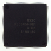
M30845FJGP#U3 Renesas Electronics America, M30845FJGP#U3 Datasheet - Page 512

M30845FJGP#U3
Manufacturer Part Number
M30845FJGP#U3
Description
IC M32C MCU FLASH 512K 144LQFP
Manufacturer
Renesas Electronics America
Series
M16C™ M32C/80r
Specifications of M30845FJGP#U3
Core Processor
M32C/80
Core Size
16/32-Bit
Speed
32MHz
Connectivity
CAN, I²C, IEBus, SIO, UART/USART
Peripherals
DMA, PWM, WDT
Number Of I /o
121
Program Memory Size
512KB (512K x 8)
Program Memory Type
FLASH
Ram Size
24K x 8
Voltage - Supply (vcc/vdd)
3 V ~ 5.5 V
Data Converters
A/D 34x10b, D/A 2x8b
Oscillator Type
Internal
Operating Temperature
-40°C ~ 85°C
Package / Case
144-LQFP
Lead Free Status / RoHS Status
Lead free / RoHS Compliant
Eeprom Size
-
Available stocks
Company
Part Number
Manufacturer
Quantity
Price
- Current page: 512 of 531
- Download datasheet (4Mb)
M
R
R
27.14 Flash Memory Version
e
E
3
. v
J
2
0
C
27.14.1 Differences Between Flash Memory Version and Masked ROM Version
27.14.2 Boot Mode
1
9
8 /
0 .
B
Due to differences in internal ROM and layout pattern, flash memory version and masked ROM version
have varying electrical characteristics such as attributes, performance margins, noise endurance capac-
ity, and noise radiation. When switching to masked ROM version, administer system evaluation tests
equal to those held on the flash memory version.
I/O pins may not be placed in high-impedance states until internal voltage stabilizes, when power is
turned on in boot mode. Follow the procedure below to turn on power in boot mode.
1) Apply an "L" signal to the RESET and the CNV
2) Wait a minimum of 2ms after V
3) Apply an "H" signal to the CNV
4) Apply an "H" signal to the RESET pin (reset exited)
0
1
4
0
G
3
J
6
u
o r
0 -
. l
u
0
1
p
, 7
0
1
(
2
M
0
3
0
2
5
C
8 /
Page 489
, 4
M
3
2
C
8 /
f o
4
____________
4
____________
) T
9
5
CC1
SS
pin
reaches 2.7V or above (until internal voltage stabilizes)
SS
pin
27. Precautions (Flash Memory Version)
Related parts for M30845FJGP#U3
Image
Part Number
Description
Manufacturer
Datasheet
Request
R

Part Number:
Description:
KIT STARTER FOR M16C/29
Manufacturer:
Renesas Electronics America
Datasheet:

Part Number:
Description:
KIT STARTER FOR R8C/2D
Manufacturer:
Renesas Electronics America
Datasheet:

Part Number:
Description:
R0K33062P STARTER KIT
Manufacturer:
Renesas Electronics America
Datasheet:

Part Number:
Description:
KIT STARTER FOR R8C/23 E8A
Manufacturer:
Renesas Electronics America
Datasheet:

Part Number:
Description:
KIT STARTER FOR R8C/25
Manufacturer:
Renesas Electronics America
Datasheet:

Part Number:
Description:
KIT STARTER H8S2456 SHARPE DSPLY
Manufacturer:
Renesas Electronics America
Datasheet:

Part Number:
Description:
KIT STARTER FOR R8C38C
Manufacturer:
Renesas Electronics America
Datasheet:

Part Number:
Description:
KIT STARTER FOR R8C35C
Manufacturer:
Renesas Electronics America
Datasheet:

Part Number:
Description:
KIT STARTER FOR R8CL3AC+LCD APPS
Manufacturer:
Renesas Electronics America
Datasheet:

Part Number:
Description:
KIT STARTER FOR RX610
Manufacturer:
Renesas Electronics America
Datasheet:

Part Number:
Description:
KIT STARTER FOR R32C/118
Manufacturer:
Renesas Electronics America
Datasheet:

Part Number:
Description:
KIT DEV RSK-R8C/26-29
Manufacturer:
Renesas Electronics America
Datasheet:

Part Number:
Description:
KIT STARTER FOR SH7124
Manufacturer:
Renesas Electronics America
Datasheet:

Part Number:
Description:
KIT STARTER FOR H8SX/1622
Manufacturer:
Renesas Electronics America
Datasheet:

Part Number:
Description:
KIT DEV FOR SH7203
Manufacturer:
Renesas Electronics America
Datasheet:


