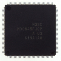
M30845FJGP#U3 Renesas Electronics America, M30845FJGP#U3 Datasheet - Page 328

M30845FJGP#U3
Manufacturer Part Number
M30845FJGP#U3
Description
IC M32C MCU FLASH 512K 144LQFP
Manufacturer
Renesas Electronics America
Series
M16C™ M32C/80r
Specifications of M30845FJGP#U3
Core Processor
M32C/80
Core Size
16/32-Bit
Speed
32MHz
Connectivity
CAN, I²C, IEBus, SIO, UART/USART
Peripherals
DMA, PWM, WDT
Number Of I /o
121
Program Memory Size
512KB (512K x 8)
Program Memory Type
FLASH
Ram Size
24K x 8
Voltage - Supply (vcc/vdd)
3 V ~ 5.5 V
Data Converters
A/D 34x10b, D/A 2x8b
Oscillator Type
Internal
Operating Temperature
-40°C ~ 85°C
Package / Case
144-LQFP
Lead Free Status / RoHS Status
Lead free / RoHS Compliant
Eeprom Size
-
Available stocks
Company
Part Number
Manufacturer
Quantity
Price
- Current page: 328 of 531
- Download datasheet (4Mb)
M
R
R
e
E
3
. v
J
2
Figure 22.25 G0ERC and G1ERC Registers
0
C
1
9
0 .
8 /
B
0
1
4
0
3
G
J
6
u
o r
0 -
. l
SI/O Expansion Receive Control Register i
b7
NOTES:
u
0
1
p
, 7
0
b6
1. The GiERC register is used in special communication mode or HDLC data processing mode.
2. When the ACRC bit in the GiEMR register is set to "1" (CRC reset function used), set the CMP3E bit
1
(
2
M
to "1".
It must be set to "0010 0000
It must be in a reset state or be set to "00
0
b5
3
0
2
5
b4
C
8 /
b3
Page 305
, 4
b2
M
3
b1
2
C
b0
f o
8 /
4
CMP1E
CMP2E
RCRCE
4
CMP0E
CMP3E
RSHTE
RBSF0
RBSF1
Symbol
) T
9
Bit
5
Symbol
G0ERC, G1ERC
2
" in clock synchronous serial I/O mode.
Receive Bit
Stuffing "1" Delete
Select Bit
Receive Bit
Stuffing "0" Delete
Select Bit
Data Compare
Function 2
Select Bit
Data Compare
Function 3
Select Bit
Receive CRC
Enable Bit
Receive Shift
Operation
Enable Bit
Data Compare
Function 0
Select Bit
Data Compare
Function 1
Select Bit
Bit Name
16
" in UART mode.
Address
00FD
0 : The GiDR register (receive data register) is
1 : The GiDR register is compared with the
0 : The GiDR register (receive data register) is
1 : The GiDR register is compared with the
0 : The GiDR register (receive data register) is
1 : The GiDR register is compared with the
0 : The GiDR register (receive data register) is
1 : The GiDR register is compared with the
0 : Not used
1 : Used
0 : Receive shift operation disabled
1 : Receive shift operation enabled
0 : "1" is not deleted
1 : "1" is deleted
0 : "0" is not deleted
1 : "0" is deleted
not compared with the GiCMP0 register
GiCMP0 register
not compared with the GiCMP1 register
GiCMP1 register
not compared with the GiCMP2 register
GiCMP2 register
not compared with the GiCMP3 register
GiCMP3 register
16
, 013D
(i=0,1)
16
22. Intelligent I/O (Communication Function)
(1)
Function
(2)
After Reset
00
16
RW
RW
RW
RW
RW
RW
RW
RW
RW
Related parts for M30845FJGP#U3
Image
Part Number
Description
Manufacturer
Datasheet
Request
R

Part Number:
Description:
KIT STARTER FOR M16C/29
Manufacturer:
Renesas Electronics America
Datasheet:

Part Number:
Description:
KIT STARTER FOR R8C/2D
Manufacturer:
Renesas Electronics America
Datasheet:

Part Number:
Description:
R0K33062P STARTER KIT
Manufacturer:
Renesas Electronics America
Datasheet:

Part Number:
Description:
KIT STARTER FOR R8C/23 E8A
Manufacturer:
Renesas Electronics America
Datasheet:

Part Number:
Description:
KIT STARTER FOR R8C/25
Manufacturer:
Renesas Electronics America
Datasheet:

Part Number:
Description:
KIT STARTER H8S2456 SHARPE DSPLY
Manufacturer:
Renesas Electronics America
Datasheet:

Part Number:
Description:
KIT STARTER FOR R8C38C
Manufacturer:
Renesas Electronics America
Datasheet:

Part Number:
Description:
KIT STARTER FOR R8C35C
Manufacturer:
Renesas Electronics America
Datasheet:

Part Number:
Description:
KIT STARTER FOR R8CL3AC+LCD APPS
Manufacturer:
Renesas Electronics America
Datasheet:

Part Number:
Description:
KIT STARTER FOR RX610
Manufacturer:
Renesas Electronics America
Datasheet:

Part Number:
Description:
KIT STARTER FOR R32C/118
Manufacturer:
Renesas Electronics America
Datasheet:

Part Number:
Description:
KIT DEV RSK-R8C/26-29
Manufacturer:
Renesas Electronics America
Datasheet:

Part Number:
Description:
KIT STARTER FOR SH7124
Manufacturer:
Renesas Electronics America
Datasheet:

Part Number:
Description:
KIT STARTER FOR H8SX/1622
Manufacturer:
Renesas Electronics America
Datasheet:

Part Number:
Description:
KIT DEV FOR SH7203
Manufacturer:
Renesas Electronics America
Datasheet:


