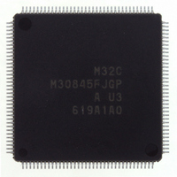
M30845FJGP#U3 Renesas Electronics America, M30845FJGP#U3 Datasheet - Page 280

M30845FJGP#U3
Manufacturer Part Number
M30845FJGP#U3
Description
IC M32C MCU FLASH 512K 144LQFP
Manufacturer
Renesas Electronics America
Series
M16C™ M32C/80r
Specifications of M30845FJGP#U3
Core Processor
M32C/80
Core Size
16/32-Bit
Speed
32MHz
Connectivity
CAN, I²C, IEBus, SIO, UART/USART
Peripherals
DMA, PWM, WDT
Number Of I /o
121
Program Memory Size
512KB (512K x 8)
Program Memory Type
FLASH
Ram Size
24K x 8
Voltage - Supply (vcc/vdd)
3 V ~ 5.5 V
Data Converters
A/D 34x10b, D/A 2x8b
Oscillator Type
Internal
Operating Temperature
-40°C ~ 85°C
Package / Case
144-LQFP
Lead Free Status / RoHS Status
Lead free / RoHS Compliant
Eeprom Size
-
Available stocks
Company
Part Number
Manufacturer
Quantity
Price
- Current page: 280 of 531
- Download datasheet (4Mb)
M
R
R
e
E
3
. v
J
2
Table 18.5 Repeat Sweep Mode 0 Specifications
0
Function
Start Condition
Stop Condition
Interrupt Request Generation Timing • When the DUS bit in the AD0CON3 register is set to "0" (DMAC operating mode
Analog Voltage Input Pins
Reading of A/D Conversion Result • When the DUS bit is set to "0", the microcomputer reads the AD0j register (j=0 to
C
18.1.4 Repeat Sweep Mode 0
1
9
8 /
0 .
B
In repeat sweep mode 0, analog voltage applied to selected pins is repeatedly converted to a digital code.
Table 18.5 lists specifications of repeat sweep mode 0.
0
1
4
0
G
3
J
6
u
o r
0 -
. l
u
0
1
p
, 7
0
Item
1
(
2
M
0
3
0
2
5
C
8 /
Page 257
, 4
M
3
2
C
8 /
f o
Select from ANi
The SCAN1 and SCAN0 bits in the AD0CON1 register and the APS1 and APS0
bits in the AD0CON2 register select pins. Analog voltage applied to the pins is
repeatedly converted to a digital code
Same as one-shot mode
The ADST bit in the AD0CON0 register is set to "0" (A/D conversion stopped) by
program
• When DUS bit is set to "1" (DMAC operating mode enabled), an interrupt request
AN
• When the DUS bit is set to "1", do not read the AD00 register. A/D conversion
4
4
disabled), no interrupt request is generated
is generated every time an A/D conversion is completed
7) corresponding to selected pins
result is stored in the AD00 register after the A/D conversion is completed.
DMAC transfers the conversion result to any memory space. Refer to 13. DMAC
for DMAC settings
) T
9
i5
5
(6 pins) or ANi
0
and ANi1 (2 pins) (i=none, 0, 2, 15), ANi
0
to ANi
7
(8 pins)
Specification
0
to ANi
3
18. A/D Converter
(4 pins), ANi
0
to
Related parts for M30845FJGP#U3
Image
Part Number
Description
Manufacturer
Datasheet
Request
R

Part Number:
Description:
KIT STARTER FOR M16C/29
Manufacturer:
Renesas Electronics America
Datasheet:

Part Number:
Description:
KIT STARTER FOR R8C/2D
Manufacturer:
Renesas Electronics America
Datasheet:

Part Number:
Description:
R0K33062P STARTER KIT
Manufacturer:
Renesas Electronics America
Datasheet:

Part Number:
Description:
KIT STARTER FOR R8C/23 E8A
Manufacturer:
Renesas Electronics America
Datasheet:

Part Number:
Description:
KIT STARTER FOR R8C/25
Manufacturer:
Renesas Electronics America
Datasheet:

Part Number:
Description:
KIT STARTER H8S2456 SHARPE DSPLY
Manufacturer:
Renesas Electronics America
Datasheet:

Part Number:
Description:
KIT STARTER FOR R8C38C
Manufacturer:
Renesas Electronics America
Datasheet:

Part Number:
Description:
KIT STARTER FOR R8C35C
Manufacturer:
Renesas Electronics America
Datasheet:

Part Number:
Description:
KIT STARTER FOR R8CL3AC+LCD APPS
Manufacturer:
Renesas Electronics America
Datasheet:

Part Number:
Description:
KIT STARTER FOR RX610
Manufacturer:
Renesas Electronics America
Datasheet:

Part Number:
Description:
KIT STARTER FOR R32C/118
Manufacturer:
Renesas Electronics America
Datasheet:

Part Number:
Description:
KIT DEV RSK-R8C/26-29
Manufacturer:
Renesas Electronics America
Datasheet:

Part Number:
Description:
KIT STARTER FOR SH7124
Manufacturer:
Renesas Electronics America
Datasheet:

Part Number:
Description:
KIT STARTER FOR H8SX/1622
Manufacturer:
Renesas Electronics America
Datasheet:

Part Number:
Description:
KIT DEV FOR SH7203
Manufacturer:
Renesas Electronics America
Datasheet:


