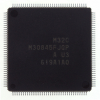
M30845FJGP#U3 Renesas Electronics America, M30845FJGP#U3 Datasheet - Page 334

M30845FJGP#U3
Manufacturer Part Number
M30845FJGP#U3
Description
IC M32C MCU FLASH 512K 144LQFP
Manufacturer
Renesas Electronics America
Series
M16C™ M32C/80r
Specifications of M30845FJGP#U3
Core Processor
M32C/80
Core Size
16/32-Bit
Speed
32MHz
Connectivity
CAN, I²C, IEBus, SIO, UART/USART
Peripherals
DMA, PWM, WDT
Number Of I /o
121
Program Memory Size
512KB (512K x 8)
Program Memory Type
FLASH
Ram Size
24K x 8
Voltage - Supply (vcc/vdd)
3 V ~ 5.5 V
Data Converters
A/D 34x10b, D/A 2x8b
Oscillator Type
Internal
Operating Temperature
-40°C ~ 85°C
Package / Case
144-LQFP
Lead Free Status / RoHS Status
Lead free / RoHS Compliant
Eeprom Size
-
Available stocks
Company
Part Number
Manufacturer
Quantity
Price
- Current page: 334 of 531
- Download datasheet (4Mb)
M
R
R
e
E
3
. v
J
2
n
NOTES:
Table 22.14 Clock Settings (Communication Unit 1)
Table 22.15 Register Settings in Clock Synchronous Serial I/O Mode (Communication Units 0 and 1)
0
C
: Setting value of the G1PO0 register, 0001
CCS
G1BCR0
G1BCR1
G1POCR0
G1POCR1
G1POCR3
G1PO0
G1PO3
G1FS
G1FE
GiERC
GiMR
GiCR
GiTB
GiRB
i = 0 to 1
NOTES:
1
9
Input from ISCLK1
1. The transfer clock is generated in phase-delayed waveform output mode of the channel 3 waveform
2. The CNT3 to CNT0 bits in the TCSPR register select no division (
3. The transfer clock must be f
0 .
8 /
B
Transfer Clock
1. The CKDIR bit in the GiMR register is set to "0" (internal clock).
2. These registers must be set, when f
Register
0
1
4
generating function.
0
3
G
(2)
(2)
J
6
u
2(
(2)
(2)
o r
f
0 -
. l
f
2n (2)
(2)
(2)
BT1
n
f
u
0
1
8
+2)
(2)
(2)
(2)
p
, 7
0
1
(
2
M
0
3
0
(3)
(1)
CCS1, CCS0
CCS3, CSS2
BCK1, BCK0
DIV4 to DIV0
IT
7 to 0
7 to 0
7 to 0
MOD2 to MOD0
IVL
RLD
INV
15 to 0
15 to 0
FSC3,FSC1,FSC0 Set to "0"
IFE3,IFE1,IFE0
7 to 0
GMD1, GMD0
CKDIR
STPS
UFORM
IRS
TI
TXEPT
RI
TE
RE
IPOL
OPOL
–
–
2
5
C
8 /
Page 311
G1MR Register
, 4
Bit
CKDIR Bit
M
3
2
0
0
0
1
C
f o
8 /
4
4
BT1
2 x (setting value + 2)
) T
Setting not required when using only
communication unit 1
Select transfer clock
Set to "11
Select divide ratio of count source
Set to "0"
Set to "0001 0010
Set to "0000 0111
Set to "0000 0111
Set to "010
Select default output value of ISCLKi
Set to "0"
Select whether ISCLKi puts in an
inversed signal or not
Set bit rate
Set to a value smaller than the G1PO0
register
Set to "1"
Set to "0010 0000
Set to "01
Select the internal clock or external clock
Set to "0"
Select either LSB first or MSB first
Select how the transmit interrupt is generated
Transmit buffer empty flag
Transmit register empty flag
Receive complete flag
Set to "1" to enable transmission and reception
Set to "1" to enable reception
Select ISRxDi input polarity (usually set to "0")
Select ISTxDi output polarity (usually set to "0")
Write data to be transmitted
Received data and error flag are stored
9
5
divided by six or more.
8
or f
(1)
Communication Unit 1
2n
f
(1)
(1)
2
2
BT1
CCS2 Bit
" (f1)
"
2
is selected as transfer clock source notwithstanding.
16
"
(1)
0
1
0
-
to FFFD
2
2
2
2
CCS Register
"
"
"
"
(1)
= transfer clock
16
frequency
CCS3 Bit
22. Intelligent I/O (Communication Function)
Function
0
1
1
-
(1)
Select transfer clock
Setting not required when using only
communication unit 0
n
=0) or divide-by-2
Communication Unit 0
n
(
n
=1 to 15).
Related parts for M30845FJGP#U3
Image
Part Number
Description
Manufacturer
Datasheet
Request
R

Part Number:
Description:
KIT STARTER FOR M16C/29
Manufacturer:
Renesas Electronics America
Datasheet:

Part Number:
Description:
KIT STARTER FOR R8C/2D
Manufacturer:
Renesas Electronics America
Datasheet:

Part Number:
Description:
R0K33062P STARTER KIT
Manufacturer:
Renesas Electronics America
Datasheet:

Part Number:
Description:
KIT STARTER FOR R8C/23 E8A
Manufacturer:
Renesas Electronics America
Datasheet:

Part Number:
Description:
KIT STARTER FOR R8C/25
Manufacturer:
Renesas Electronics America
Datasheet:

Part Number:
Description:
KIT STARTER H8S2456 SHARPE DSPLY
Manufacturer:
Renesas Electronics America
Datasheet:

Part Number:
Description:
KIT STARTER FOR R8C38C
Manufacturer:
Renesas Electronics America
Datasheet:

Part Number:
Description:
KIT STARTER FOR R8C35C
Manufacturer:
Renesas Electronics America
Datasheet:

Part Number:
Description:
KIT STARTER FOR R8CL3AC+LCD APPS
Manufacturer:
Renesas Electronics America
Datasheet:

Part Number:
Description:
KIT STARTER FOR RX610
Manufacturer:
Renesas Electronics America
Datasheet:

Part Number:
Description:
KIT STARTER FOR R32C/118
Manufacturer:
Renesas Electronics America
Datasheet:

Part Number:
Description:
KIT DEV RSK-R8C/26-29
Manufacturer:
Renesas Electronics America
Datasheet:

Part Number:
Description:
KIT STARTER FOR SH7124
Manufacturer:
Renesas Electronics America
Datasheet:

Part Number:
Description:
KIT STARTER FOR H8SX/1622
Manufacturer:
Renesas Electronics America
Datasheet:

Part Number:
Description:
KIT DEV FOR SH7203
Manufacturer:
Renesas Electronics America
Datasheet:


