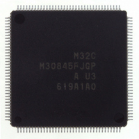
M30845FJGP#U3 Renesas Electronics America, M30845FJGP#U3 Datasheet - Page 500

M30845FJGP#U3
Manufacturer Part Number
M30845FJGP#U3
Description
IC M32C MCU FLASH 512K 144LQFP
Manufacturer
Renesas Electronics America
Series
M16C™ M32C/80r
Specifications of M30845FJGP#U3
Core Processor
M32C/80
Core Size
16/32-Bit
Speed
32MHz
Connectivity
CAN, I²C, IEBus, SIO, UART/USART
Peripherals
DMA, PWM, WDT
Number Of I /o
121
Program Memory Size
512KB (512K x 8)
Program Memory Type
FLASH
Ram Size
24K x 8
Voltage - Supply (vcc/vdd)
3 V ~ 5.5 V
Data Converters
A/D 34x10b, D/A 2x8b
Oscillator Type
Internal
Operating Temperature
-40°C ~ 85°C
Package / Case
144-LQFP
Lead Free Status / RoHS Status
Lead free / RoHS Compliant
Eeprom Size
-
Available stocks
Company
Part Number
Manufacturer
Quantity
Price
- Current page: 500 of 531
- Download datasheet (4Mb)
M
R
R
e
E
3
27.7 Interrupts
. v
J
2
Figure 27.3 Switching Procedure for INT Interrupt
0
C
27.7.1 ISP Setting
27.7.2 NMI Interrupt
27.7.3 INT Interrupt
1
9
8 /
0 .
B
After reset, the ISP is set to "000000
before the ISP is set. Therefore, the ISP must be set before an interrupt request is generated. Set the ISP
to an even address, which allows interrupt sequences to be executed at a higher speed.
To use NMI interrupt, set the ISP at the beginning of the program. The NMI interrupt can be acknowl-
edged after the first instruction has been executed after reset.
• NMI interrupt cannot be denied. Connect the NMI pin to V
• The P8_5 bit in the P8 register indicates the NMI pin value. Read the P8_5 bit only to determine the pin
• "H" and "L" signals applied to the NMI pin must be over 2 CPU clock cycles + 300 ns wide.
• NMI interrupt request may not be acknowledged if this and other interrupt requests are generated
• Edge Sensitive
• Level Sensitive
• The IR bit may change to "1" (interrupt requested) when switching the polarity of the INT0 to INT5 pins.
0
1
4
_______
level after a NMI interrupt occurs.
simultaneously.
Set the IR bit to "0" (no interrupt requested) after selecting the polarity. Figure 27.3 shows an example of
the switching procedure for the INT interrupt.
_______
clock.
"H" and "L" signals applied to the INT0 to INT5 pins must be at least 250 ns wide, regardless of the CPU
"H" and "L" signals applied to the INT0 to INT5 pins must be at least 1 CPU clock cycle + 200 ns wide.
0
For example, "H" and "L" must be at least 234ns wide if X
G
3
J
6
u
o r
0 -
. l
u
_______
______
0
1
_______
p
, 7
0
1
(
2
M
0
3
0
_______
2
5
C
8 /
Page 477
, 4
M
3
2
C
Set the ILVL2 to ILVL0 bits to "001
to "111
(INT interrupt request acknowledgement enabled)
8 /
f o
Set the ILVL2 to ILVL0 bits in the INTiIC
register (i = 0 to 5) to "000
4
4
Set the IR bit in the INTiIC register to "0"
) T
9
Set the POL bit in the INTiIC register
5
2
" (level 7)
______
______
_______
______
16
______
". The program runs out of control if an interrupt is acknowledged
(
INT
______
interrupt disabled)
______
_______
_______
2
" (level 0)
2
CC
IN
" (level 1)
=30MHz with no division.
via a resistor (pull-up) when not in use.
_______
27. Precautions (Interrupts)
______
______
Related parts for M30845FJGP#U3
Image
Part Number
Description
Manufacturer
Datasheet
Request
R

Part Number:
Description:
KIT STARTER FOR M16C/29
Manufacturer:
Renesas Electronics America
Datasheet:

Part Number:
Description:
KIT STARTER FOR R8C/2D
Manufacturer:
Renesas Electronics America
Datasheet:

Part Number:
Description:
R0K33062P STARTER KIT
Manufacturer:
Renesas Electronics America
Datasheet:

Part Number:
Description:
KIT STARTER FOR R8C/23 E8A
Manufacturer:
Renesas Electronics America
Datasheet:

Part Number:
Description:
KIT STARTER FOR R8C/25
Manufacturer:
Renesas Electronics America
Datasheet:

Part Number:
Description:
KIT STARTER H8S2456 SHARPE DSPLY
Manufacturer:
Renesas Electronics America
Datasheet:

Part Number:
Description:
KIT STARTER FOR R8C38C
Manufacturer:
Renesas Electronics America
Datasheet:

Part Number:
Description:
KIT STARTER FOR R8C35C
Manufacturer:
Renesas Electronics America
Datasheet:

Part Number:
Description:
KIT STARTER FOR R8CL3AC+LCD APPS
Manufacturer:
Renesas Electronics America
Datasheet:

Part Number:
Description:
KIT STARTER FOR RX610
Manufacturer:
Renesas Electronics America
Datasheet:

Part Number:
Description:
KIT STARTER FOR R32C/118
Manufacturer:
Renesas Electronics America
Datasheet:

Part Number:
Description:
KIT DEV RSK-R8C/26-29
Manufacturer:
Renesas Electronics America
Datasheet:

Part Number:
Description:
KIT STARTER FOR SH7124
Manufacturer:
Renesas Electronics America
Datasheet:

Part Number:
Description:
KIT STARTER FOR H8SX/1622
Manufacturer:
Renesas Electronics America
Datasheet:

Part Number:
Description:
KIT DEV FOR SH7203
Manufacturer:
Renesas Electronics America
Datasheet:


