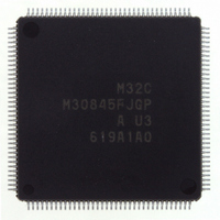
M30845FJGP#U3 Renesas Electronics America, M30845FJGP#U3 Datasheet - Page 522

M30845FJGP#U3
Manufacturer Part Number
M30845FJGP#U3
Description
IC M32C MCU FLASH 512K 144LQFP
Manufacturer
Renesas Electronics America
Series
M16C™ M32C/80r
Specifications of M30845FJGP#U3
Core Processor
M32C/80
Core Size
16/32-Bit
Speed
32MHz
Connectivity
CAN, I²C, IEBus, SIO, UART/USART
Peripherals
DMA, PWM, WDT
Number Of I /o
121
Program Memory Size
512KB (512K x 8)
Program Memory Type
FLASH
Ram Size
24K x 8
Voltage - Supply (vcc/vdd)
3 V ~ 5.5 V
Data Converters
A/D 34x10b, D/A 2x8b
Oscillator Type
Internal
Operating Temperature
-40°C ~ 85°C
Package / Case
144-LQFP
Lead Free Status / RoHS Status
Lead free / RoHS Compliant
Eeprom Size
-
Available stocks
Company
Part Number
Manufacturer
Quantity
Price
- Current page: 522 of 531
- Download datasheet (4Mb)
Rev.
REVISION HISTORY
Date
Page
101
103
104
107
109
111
116
117
119
120
121
122
123
131
132
137
138
147
153
154
155
160
175
96
98
99
• Table 9.6 CLK
• 9.5.2 Wait Mode Chapter structure modified
• Table 9.7 Pin States in Wait Mode Note 1 added
• 9.5.3 Stop Mode Interrupt usable to exit stop mode added; note 1 added
• Table 9.9 Pin Status in Stop Mode Note 1 added
• Figure 9.13 Status Transition in Wait Mode and Stop Mode Figure partially
• Figure 9.14 Status Transition Note 5 modified
Interrupts
• Figure 11.1 Interrupts Note 3 added
• Figure 11.1 Interrupts Note 3 added
• 11.3.1.4 Low Voltage Detection Interrupt Note 1 added
• Figure 11.4 Interrupt Control Register (2) Note mark position changed
• Figure 11.5 RLVL Register Value after reset changed; note 4 deleted
• 11.6.4 Interrupt Response Time Description modified
• Figure 11.5 Interrupts without Interrupt Priority Levels and IPL Note1 added
• 11.6.6 Saving a Register Description modified; note1 added
• Figure 11.8 Interrupt Priority Note 1 added
• Figure 11.9 Interrupt Priority Level Select Circuit Note 1 added
Watchdog Timer
• Figure 12.1 Watchdog Timer Block Diagram Block diagram modified
• Figure 12.2 WDC Register and WDTS Register Note 3 added to the WDC
DMAC
• Figure 13.2 DM0SL to DM3SL Registers Value after reset changed
• Table 13.2 DMiSL Register (i=0 to 3) Function Note 3 modified
DMACII
• Figure 14.1 RLVL Register Value after reset changed; note 4 deleted
• 14.8 Execution Time Description modified
• Figure 14.5 Transfer Cycle The number of cycles changed
Timer
• Figure 15.1 Timer A Configuration Figure modified
• Figure 15.2 Timer B Configuration Figure modified
• Figure 15.7 TRGSR Register and TCSPR Register Added note 2 to the
• Table 15.8 Settings for the TBi
Mode Note 4 added
modified; Note 2 deleted; Note numbers changed accordingly
register
TCSPR register
modified
M32C/84 Group(M32C/84, M32C/84T) Hardware Manual
OUT
Pin in Memory Expansion Mode and Microprocessor
C-4
Description
IN
Summary
Pins (i=0 to 5) PS3 bit in the P9
4
register
Related parts for M30845FJGP#U3
Image
Part Number
Description
Manufacturer
Datasheet
Request
R

Part Number:
Description:
KIT STARTER FOR M16C/29
Manufacturer:
Renesas Electronics America
Datasheet:

Part Number:
Description:
KIT STARTER FOR R8C/2D
Manufacturer:
Renesas Electronics America
Datasheet:

Part Number:
Description:
R0K33062P STARTER KIT
Manufacturer:
Renesas Electronics America
Datasheet:

Part Number:
Description:
KIT STARTER FOR R8C/23 E8A
Manufacturer:
Renesas Electronics America
Datasheet:

Part Number:
Description:
KIT STARTER FOR R8C/25
Manufacturer:
Renesas Electronics America
Datasheet:

Part Number:
Description:
KIT STARTER H8S2456 SHARPE DSPLY
Manufacturer:
Renesas Electronics America
Datasheet:

Part Number:
Description:
KIT STARTER FOR R8C38C
Manufacturer:
Renesas Electronics America
Datasheet:

Part Number:
Description:
KIT STARTER FOR R8C35C
Manufacturer:
Renesas Electronics America
Datasheet:

Part Number:
Description:
KIT STARTER FOR R8CL3AC+LCD APPS
Manufacturer:
Renesas Electronics America
Datasheet:

Part Number:
Description:
KIT STARTER FOR RX610
Manufacturer:
Renesas Electronics America
Datasheet:

Part Number:
Description:
KIT STARTER FOR R32C/118
Manufacturer:
Renesas Electronics America
Datasheet:

Part Number:
Description:
KIT DEV RSK-R8C/26-29
Manufacturer:
Renesas Electronics America
Datasheet:

Part Number:
Description:
KIT STARTER FOR SH7124
Manufacturer:
Renesas Electronics America
Datasheet:

Part Number:
Description:
KIT STARTER FOR H8SX/1622
Manufacturer:
Renesas Electronics America
Datasheet:

Part Number:
Description:
KIT DEV FOR SH7203
Manufacturer:
Renesas Electronics America
Datasheet:


