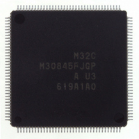
M30845FJGP#U3 Renesas Electronics America, M30845FJGP#U3 Datasheet - Page 520

M30845FJGP#U3
Manufacturer Part Number
M30845FJGP#U3
Description
IC M32C MCU FLASH 512K 144LQFP
Manufacturer
Renesas Electronics America
Series
M16C™ M32C/80r
Specifications of M30845FJGP#U3
Core Processor
M32C/80
Core Size
16/32-Bit
Speed
32MHz
Connectivity
CAN, I²C, IEBus, SIO, UART/USART
Peripherals
DMA, PWM, WDT
Number Of I /o
121
Program Memory Size
512KB (512K x 8)
Program Memory Type
FLASH
Ram Size
24K x 8
Voltage - Supply (vcc/vdd)
3 V ~ 5.5 V
Data Converters
A/D 34x10b, D/A 2x8b
Oscillator Type
Internal
Operating Temperature
-40°C ~ 85°C
Package / Case
144-LQFP
Lead Free Status / RoHS Status
Lead free / RoHS Compliant
Eeprom Size
-
Available stocks
Company
Part Number
Manufacturer
Quantity
Price
- Current page: 520 of 531
- Download datasheet (4Mb)
Rev.
REVISION HISTORY
Date
8-10,13,14 • Tables 1.4 and 1.5 Pin Characteristics for 144-Pin Package/ for 100-Pin
Page
7, 12
2, 3
15
22
24
26
29
35
37
38
41
43
44
45
23
4
5
6
-
• Tables 1.1 and 1.2 M32C/84 Group (M32C/84, M32C/84T) Performance M32C/
• 1.3 Block Diagram Description deleted
• Figure 1.1 M32C/84 Group (M32C/84, M32C/84T) Block Diagram; Note 3
• 1.4 Product Information Description modified; ROM/RAM Capacity deleted
• Table 1.3 M32C/84 Group (M32C/84, M32C/84T) Information updated; M32C/
• Figure 1.2 Product Numbering System Classification modified
• Figures 1.3 and 1.5 Pin Assignment for 144-Pin Package/ for 100-Pin Package
• Tables 1.6 Pin Characteristics for 100-Pin and 144-Pin Package Notes 2 and
Memory
• Figure 3.1 Memory Map Type number table modified; note 2 modified; notes 4
SFR
• The DS, VCR2, VCR1 and D4INT registers Note 2 added
• The EWCR0 to EWCR3 registers Note 1 added
• The RMR0 register Value after reset added
• The RLVL register Value after reset modified
• The G1RB register Value after reset modified
• The IDB1 and IDB0 registers Value after reset modified
• The DM3SL to DM0SL registers Value after reset modified
• The A/D0 register Symbol name modified
• The PSC register Value after reset modified
Reset
• Hardware Reset 2 changed to Voltage Down Detection Reset
• Chapter structure modified
• 5. Reset Hardware Reset 1 and Voltage Down Detection Reset added to description
• 5.1 Hardware Reset Section deleted
• Figure 5.1 Reset Circuit Note 1 modified
• Figure 5.2 Reset Sequence Figure modified; Notes 1, 2, and 3 added
• Table 5.1 Pin State while RESET Pin is Held "L" Note 3 added to P5
• 5.2 Voltage Down Detection Reset td(P-R) changed to td(S-R); Note 1 added
84T added; supply voltage on Power Consumption row modified; note 3 and 4
added
added
84T added
Note 3/Note 5 added
Package Notes 2 and 3 added
3 added
and 5 added
M32C/84 Group(M32C/84, M32C/84T) Hardware Manual
C-2
Description
Summary
6
Related parts for M30845FJGP#U3
Image
Part Number
Description
Manufacturer
Datasheet
Request
R

Part Number:
Description:
KIT STARTER FOR M16C/29
Manufacturer:
Renesas Electronics America
Datasheet:

Part Number:
Description:
KIT STARTER FOR R8C/2D
Manufacturer:
Renesas Electronics America
Datasheet:

Part Number:
Description:
R0K33062P STARTER KIT
Manufacturer:
Renesas Electronics America
Datasheet:

Part Number:
Description:
KIT STARTER FOR R8C/23 E8A
Manufacturer:
Renesas Electronics America
Datasheet:

Part Number:
Description:
KIT STARTER FOR R8C/25
Manufacturer:
Renesas Electronics America
Datasheet:

Part Number:
Description:
KIT STARTER H8S2456 SHARPE DSPLY
Manufacturer:
Renesas Electronics America
Datasheet:

Part Number:
Description:
KIT STARTER FOR R8C38C
Manufacturer:
Renesas Electronics America
Datasheet:

Part Number:
Description:
KIT STARTER FOR R8C35C
Manufacturer:
Renesas Electronics America
Datasheet:

Part Number:
Description:
KIT STARTER FOR R8CL3AC+LCD APPS
Manufacturer:
Renesas Electronics America
Datasheet:

Part Number:
Description:
KIT STARTER FOR RX610
Manufacturer:
Renesas Electronics America
Datasheet:

Part Number:
Description:
KIT STARTER FOR R32C/118
Manufacturer:
Renesas Electronics America
Datasheet:

Part Number:
Description:
KIT DEV RSK-R8C/26-29
Manufacturer:
Renesas Electronics America
Datasheet:

Part Number:
Description:
KIT STARTER FOR SH7124
Manufacturer:
Renesas Electronics America
Datasheet:

Part Number:
Description:
KIT STARTER FOR H8SX/1622
Manufacturer:
Renesas Electronics America
Datasheet:

Part Number:
Description:
KIT DEV FOR SH7203
Manufacturer:
Renesas Electronics America
Datasheet:


