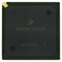
MPC561MZP56 Freescale Semiconductor, MPC561MZP56 Datasheet - Page 838

MPC561MZP56
Manufacturer Part Number
MPC561MZP56
Description
IC MPU 32BIT 56MHZ PPC 388-PBGA
Manufacturer
Freescale Semiconductor
Series
MPC5xxr
Datasheet
1.MPC561MZP56.pdf
(1420 pages)
Specifications of MPC561MZP56
Core Processor
PowerPC
Core Size
32-Bit
Speed
56MHz
Connectivity
CAN, EBI/EMI, SCI, SPI, UART/USART
Peripherals
POR, PWM, WDT
Number Of I /o
64
Program Memory Type
ROMless
Ram Size
32K x 8
Voltage - Supply (vcc/vdd)
2.5 V ~ 2.7 V
Data Converters
A/D 32x10b
Oscillator Type
External
Operating Temperature
-40°C ~ 125°C
Package / Case
388-BGA
Controller Family/series
POWER 5xx
No. Of I/o's
56
Ram Memory Size
31KB
Cpu Speed
56MHz
No. Of Timers
32
Embedded Interface Type
QSPI, SCI, UART
No. Of Pwm Channels
12
Rohs Compliant
No
Processor Series
MPC5xx
Core
PowerPC
Data Bus Width
32 bit
Data Ram Size
32 KB
Interface Type
CAN, JTAG, QSPI, SCI, SPI, UART
Maximum Clock Frequency
40 MHz
Number Of Programmable I/os
56
Number Of Timers
22
Operating Supply Voltage
2.6 V to 5 V
Maximum Operating Temperature
+ 85 C
Mounting Style
SMD/SMT
Minimum Operating Temperature
- 40 C
On-chip Adc
2 (10 bit, 32 Channel)
For Use With
MPC564EVB - KIT EVAL FOR MPC561/562/563/564
Lead Free Status / RoHS Status
Contains lead / RoHS non-compliant
Eeprom Size
-
Program Memory Size
-
Lead Free Status / Rohs Status
No
Available stocks
Company
Part Number
Manufacturer
Quantity
Price
Company:
Part Number:
MPC561MZP56
Manufacturer:
Freescale Semiconductor
Quantity:
10 000
Company:
Part Number:
MPC561MZP56R2
Manufacturer:
Freescale Semiconductor
Quantity:
10 000
- Current page: 838 of 1420
- Download datasheet (11Mb)
Time Processor Unit 3
Table 19-5
prescaler).
19.4
The TPU3 memory map contains three groups of registers:
All registers except the channel interrupt status register (CISR) must be read or written by means of
half-word (16-bit) or word (32-bit) accesses. The address space of the TPU3 memory map occupies 512
bytes. Unused registers within the 512-byte address space return zeros when read.
Table 19-6
19-8
•
•
•
System configuration registers
Channel control and status registers
Development support and test verification registers
TCR2 Value
TCR2PSCK2
CLOCK
DIV8
TCR2
Pin
Programming Model
is a summary of prescaler output (assuming a divide-by-one value for the pre-divider
shows the TPU3 address map.
0b00
0b01
0b10
0b11
0x30 4000(TPU_A)
0x30 4400(TPU_B)
0x30 4002(TPU_A)
0x30 4402(TPU_B)
0x30 4004(TPU_A)
0x30 4404(TPU_B)
0x30 4006(TPU_A)
0x30 4406(TPU_B)
Address
Control
TCR2PSCK2 = 0
Mux
Internal Clock Divide Ratio
16
32
64
8
MPC561/MPC563 Reference Manual, Rev. 1.2
Figure 19-4. TCR2 Prescaler Control
Table 19-5. TCR2 Prescaler Control
Clock
Source
Table 19-6. TPU3 Register Map
TPU3 Module Configuration Register (TPUMCR)
See
TPU3 Test Configuration Register (TCR)
Development Support Control Register (DSCR)
See
Development Support Status Register (DSSR)
See
Table 19-7
Table 19-8
Table 19-9
TCR2PSCK2 = 1
Pre-divider
Prescaler
120
24
56
8
for bit descriptions.
for bit descriptions.
for bit descriptions.
Register
TCR2PSCK2 = 0
Prescaler
TCR2
External Clock Divide Ratio
1
2
4
8
Freescale Semiconductor
TCR2PSCK2 = 1
TCR2
15
1
3
7
Related parts for MPC561MZP56
Image
Part Number
Description
Manufacturer
Datasheet
Request
R

Part Number:
Description:
MPC5 1K0 5%
Manufacturer:
TE Connectivity
Datasheet:

Part Number:
Description:
MPC5 500R 5%
Manufacturer:
TE Connectivity
Datasheet:

Part Number:
Description:
MPC5 5K0 5%
Manufacturer:
Tyco Electronics
Datasheet:

Part Number:
Description:
MPC5 5R0 5%
Manufacturer:
Tyco Electronics
Datasheet:

Part Number:
Description:
MPC5 50K 5%
Manufacturer:
Tyco Electronics
Datasheet:

Part Number:
Description:
MPC5 1R0 5%
Manufacturer:
Tyco Electronics
Datasheet:
Part Number:
Description:
Manufacturer:
Freescale Semiconductor, Inc
Datasheet:
Part Number:
Description:
Manufacturer:
Freescale Semiconductor, Inc
Datasheet:
Part Number:
Description:
Manufacturer:
Freescale Semiconductor, Inc
Datasheet:
Part Number:
Description:
Manufacturer:
Freescale Semiconductor, Inc
Datasheet:
Part Number:
Description:
Manufacturer:
Freescale Semiconductor, Inc
Datasheet:


