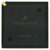
MPC561MZP56 Freescale Semiconductor, MPC561MZP56 Datasheet - Page 1243

MPC561MZP56
Manufacturer Part Number
MPC561MZP56
Description
IC MPU 32BIT 56MHZ PPC 388-PBGA
Manufacturer
Freescale Semiconductor
Series
MPC5xxr
Datasheet
1.MPC561MZP56.pdf
(1420 pages)
Specifications of MPC561MZP56
Core Processor
PowerPC
Core Size
32-Bit
Speed
56MHz
Connectivity
CAN, EBI/EMI, SCI, SPI, UART/USART
Peripherals
POR, PWM, WDT
Number Of I /o
64
Program Memory Type
ROMless
Ram Size
32K x 8
Voltage - Supply (vcc/vdd)
2.5 V ~ 2.7 V
Data Converters
A/D 32x10b
Oscillator Type
External
Operating Temperature
-40°C ~ 125°C
Package / Case
388-BGA
Controller Family/series
POWER 5xx
No. Of I/o's
56
Ram Memory Size
31KB
Cpu Speed
56MHz
No. Of Timers
32
Embedded Interface Type
QSPI, SCI, UART
No. Of Pwm Channels
12
Rohs Compliant
No
Processor Series
MPC5xx
Core
PowerPC
Data Bus Width
32 bit
Data Ram Size
32 KB
Interface Type
CAN, JTAG, QSPI, SCI, SPI, UART
Maximum Clock Frequency
40 MHz
Number Of Programmable I/os
56
Number Of Timers
22
Operating Supply Voltage
2.6 V to 5 V
Maximum Operating Temperature
+ 85 C
Mounting Style
SMD/SMT
Minimum Operating Temperature
- 40 C
On-chip Adc
2 (10 bit, 32 Channel)
For Use With
MPC564EVB - KIT EVAL FOR MPC561/562/563/564
Lead Free Status / RoHS Status
Contains lead / RoHS non-compliant
Eeprom Size
-
Program Memory Size
-
Lead Free Status / Rohs Status
No
Available stocks
Company
Part Number
Manufacturer
Quantity
Price
Company:
Part Number:
MPC561MZP56
Manufacturer:
Freescale Semiconductor
Quantity:
10 000
Company:
Part Number:
MPC561MZP56R2
Manufacturer:
Freescale Semiconductor
Quantity:
10 000
- Current page: 1243 of 1420
- Download datasheet (11Mb)
Note: (V
Freescale Semiconductor
CLKOUT
DD
= 2.6 V ± 0.1 V, V
1
2
3
4
5
29
30
56-MHz operation is available as an option. Some parts (without the 56-MHz option) will operate at a
maximum frequency of 40 MHz.
The timing for BR output is relevant when the MPC561/MPC563 is
selected to work with external bus arbiter. The timing for BG output is relevant when the
MPC561/MPC563 is selected to work with internal bus arbiter.
The setup times required for TA, TEA, and BI are relevant only when they are supplied by the external
device (and not the memory controller).
The maximum value of spec 8 for DATA[0:31] pins must be extended by 1.1 ns if the pins have been
precharged to greater than V
the max. value of VDATAPC. This is currently specified at 3.1 V. The 1.1 ns addition to spec 8 reflects
the expected timing degradation for 3.1 V.
The timing 27 refers to CS when ACS = ‘00’ and to WE[0:3]/BE[0:3] when CSNT = ‘0’.
The D[0:31] input timings 17 and 18 refer to the rising edge of the CLKOUT
in which the TA input signal is asserted.
TS valid to CLKOUT Rising
Edge (Setup Time)
CLKOUT Rising Edge to TS
Valid (Hold Time).
Characteristic
DDH
= 5.0 V ± 0.25 V, T
Table F-10. Bus Operation Timing (continued)
MPC561/MPC563 Reference Manual, Rev. 1.2
5
4
DDL
Figure F-10. CLKOUT Pin Timing
. This is the case if an external slave device on the bus is running at
A
= T
Min
L
7
5
NOTE
to T
40 MHz
H
, 50 pF load unless noted otherwise)
Max
3
Min
1
5
5
56 MHz
2
1
Max
Electrical Characteristics
Unit
ns
ns
F-27
Related parts for MPC561MZP56
Image
Part Number
Description
Manufacturer
Datasheet
Request
R

Part Number:
Description:
MPC5 1K0 5%
Manufacturer:
TE Connectivity
Datasheet:

Part Number:
Description:
MPC5 500R 5%
Manufacturer:
TE Connectivity
Datasheet:

Part Number:
Description:
MPC5 5K0 5%
Manufacturer:
Tyco Electronics
Datasheet:

Part Number:
Description:
MPC5 5R0 5%
Manufacturer:
Tyco Electronics
Datasheet:

Part Number:
Description:
MPC5 50K 5%
Manufacturer:
Tyco Electronics
Datasheet:

Part Number:
Description:
MPC5 1R0 5%
Manufacturer:
Tyco Electronics
Datasheet:
Part Number:
Description:
Manufacturer:
Freescale Semiconductor, Inc
Datasheet:
Part Number:
Description:
Manufacturer:
Freescale Semiconductor, Inc
Datasheet:
Part Number:
Description:
Manufacturer:
Freescale Semiconductor, Inc
Datasheet:
Part Number:
Description:
Manufacturer:
Freescale Semiconductor, Inc
Datasheet:
Part Number:
Description:
Manufacturer:
Freescale Semiconductor, Inc
Datasheet:


