HD64F2612FA20 Renesas Electronics America, HD64F2612FA20 Datasheet - Page 519
HD64F2612FA20
Manufacturer Part Number
HD64F2612FA20
Description
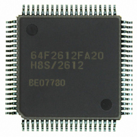
IC H8S MCU FLASH 128K 80QFP
Manufacturer
Renesas Electronics America
Series
H8® H8S/2600r
Specifications of HD64F2612FA20
Core Processor
H8S/2600
Core Size
16-Bit
Speed
20MHz
Connectivity
CAN, SCI
Peripherals
POR, PWM, WDT
Number Of I /o
43
Program Memory Size
128KB (128K x 8)
Program Memory Type
FLASH
Ram Size
4K x 8
Voltage - Supply (vcc/vdd)
4.5 V ~ 5.5 V
Data Converters
A/D 12x10b
Oscillator Type
Internal
Operating Temperature
-20°C ~ 75°C
Package / Case
80-QFP
Lead Free Status / RoHS Status
Contains lead / RoHS non-compliant
Eeprom Size
-
Available stocks
Company
Part Number
Manufacturer
Quantity
Price

Part Number:
HD64F2612FA20
Manufacturer:
RENESAS/瑞萨
Quantity:
20 000
Part Number:
HD64F2612FA20J
Manufacturer:
RENESAS/瑞萨
Quantity:
20 000


19.3
The PLL circuit multiplies the frequency of the clock from the oscillator by a factor of 1, 2, or 4.
The multiplication factor is set by the STC0 bit and the STC1 bit in LPWRCR. The phase of the
rising edge of the internal clock is controlled so as to match that at the EXTAL pin.
When the multiplication factor of the PLL circuit is changed, the operation varies according to the
setting of the STCS bit in SCKCR.
When STCS = 0, the setting becomes valid after a transition to software standby mode. The
transition time count is performed in accordance with the setting of bits STS0 to STS2 in SBYCR.
For details on SBYCR, refer to section 20.1.1, Standby Control Register (SBYCR).
1. The initial PLL circuit multiplication factor is 1.
2. STS0 to STS2 are set to give the specified transition time.
3. The target value is set in STC0 and STC1, and a transition is made to software standby mode.
4. The clock pulse generator stops and the value set in STC0 and STC1 becomes valid.
5. Software standby mode is cleared, and a transition time is secured in accordance with the
6. After the set transition time has elapsed, this LSI resumes operation using the target
If a PC break is set for the SLEEP instruction, software standby mode is entered and break
exception handling is executed after the oscillation stabilization time. In this case, the instruction
following the SLEEP instruction is executed after execution of the RTE instruction. When STCS =
1, this LSI operates on the changed multiplication factor immediately after bits STC0 and STC1
are rewritten.
19.4
The medium-speed clock divider divides the system clock to generate φ/2, φ/4, φ/8, φ/16, and φ/32.
19.5
The bus master clock selection circuit selects the clock supplied to the bus master by setting the
bits SCK 2 to SCK 0 in SCKCR. The bus master clock can be selected from high-speed mode, or
medium-speed clocks (φ/2, φ/4, φ/8, φ/16, φ/32).
setting in STS0 to STS2.
multiplication factor.
PLL Circuit
Medium-Speed Clock Divider
Bus Master Clock Selection Circuit
Rev. 7.00 Sep. 11, 2009 Page 483 of 566
Section 19 Clock Pulse Generator
REJ09B0211-0700
Related parts for HD64F2612FA20
Image
Part Number
Description
Manufacturer
Datasheet
Request
R


Part Number:
Description:
KIT STARTER FOR M16C/29
Manufacturer:
Renesas Electronics America
Datasheet:

Part Number:
Description:
KIT STARTER FOR R8C/2D
Manufacturer:
Renesas Electronics America
Datasheet:

Part Number:
Description:
R0K33062P STARTER KIT
Manufacturer:
Renesas Electronics America
Datasheet:

Part Number:
Description:
KIT STARTER FOR R8C/23 E8A
Manufacturer:
Renesas Electronics America
Datasheet:

Part Number:
Description:
KIT STARTER FOR R8C/25
Manufacturer:
Renesas Electronics America
Datasheet:

Part Number:
Description:
KIT STARTER H8S2456 SHARPE DSPLY
Manufacturer:
Renesas Electronics America
Datasheet:

Part Number:
Description:
KIT STARTER FOR R8C38C
Manufacturer:
Renesas Electronics America
Datasheet:

Part Number:
Description:
KIT STARTER FOR R8C35C
Manufacturer:
Renesas Electronics America
Datasheet:

Part Number:
Description:
KIT STARTER FOR R8CL3AC+LCD APPS
Manufacturer:
Renesas Electronics America
Datasheet:
Part Number:
Description:
KIT STARTER FOR RX610
Manufacturer:
Renesas Electronics America
Datasheet:

Part Number:
Description:
KIT STARTER FOR R32C/118
Manufacturer:
Renesas Electronics America
Datasheet:

Part Number:
Description:
KIT DEV RSK-R8C/26-29
Manufacturer:
Renesas Electronics America
Datasheet:

Part Number:
Description:
KIT STARTER FOR SH7124
Manufacturer:
Renesas Electronics America
Datasheet:

Part Number:
Description:
KIT STARTER FOR H8SX/1622
Manufacturer:
Renesas Electronics America
Datasheet: