HD64F2612FA20 Renesas Electronics America, HD64F2612FA20 Datasheet - Page 308
HD64F2612FA20
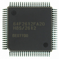
Manufacturer Part Number
HD64F2612FA20
Description
IC H8S MCU FLASH 128K 80QFP
Manufacturer
Renesas Electronics America
Series
H8® H8S/2600r
Specifications of HD64F2612FA20
Core Processor
H8S/2600
Core Size
16-Bit
Speed
20MHz
Connectivity
CAN, SCI
Peripherals
POR, PWM, WDT
Number Of I /o
43
Program Memory Size
128KB (128K x 8)
Program Memory Type
FLASH
Ram Size
4K x 8
Voltage - Supply (vcc/vdd)
4.5 V ~ 5.5 V
Data Converters
A/D 12x10b
Oscillator Type
Internal
Operating Temperature
-20°C ~ 75°C
Package / Case
80-QFP
Lead Free Status / RoHS Status
Contains lead / RoHS non-compliant
Eeprom Size
-
Available stocks
Company
Part Number
Manufacturer
Quantity
Price

Part Number:
HD64F2612FA20
Manufacturer:
RENESAS/瑞萨
Quantity:
20 000
Part Number:
HD64F2612FA20J
Manufacturer:
RENESAS/瑞萨
Quantity:
20 000


Section 11 Motor Management Timer (MMT)
Writing to Timer General Register U (TGRU), Timer General Register V (TGRV), Timer
General Register W (TGRW): Pay attention to the notices below, when a value is written into
the Timer General Register U (TGRU), Timer General Register V (TGRV), Timer General
Register W (TGRW), and in case of written into free operation address * .
• In case of Count UP: Do not write a value “Previous value of TGRU + Td” into TGRU.
• In case of Count DOWN: Do not write a value “Previous value of TGRU + Td” into TGRU.
In the same manner to TGRV, and TGRW. When a value “Previous value of TGRU + Td” is
written (in case of Count DOWN “Previous value of TGRU – Td”), the output of PUOA/PUOB,
PVOA/PVOB, PWOA/PWOB (corresponding to U, V, W phase may not be output for 1 cycle.
Figure 11.19 shows the error case.
This note is not applied when a value is written into buffer operation address.
Note: When address, H'FFFF049C, H'FFFF04AC, H'FFFF04BC are used as register address for
Previous value of TGRU
Writing to Timer Period Data Register (TPDR), and Timer Dead Time Data Register
(TDDR):
• Do not revise TPDR register when MMT is operating. Always use a buffer-write operation
• Do not revise TDDR register once an operation of MMT is invoked. When TDDR is revised, a
Rev. 7.00 Sep. 11, 2009 Page 272 of 566
REJ09B0211-0700
through TPBR register.
wave may not be output for as much as 1 cycle (full count period of 16 bits in TDCNT),
because a value cannot be written into TDCNT, which is compared to a value set in TDDR.
TBRU, TBRV, TBRW, respectively.
TGRU
2Td
Td
Figure 11.19 Error Case in Writing Operation
Case of count Up
Previous value of TGRU
TGRU
2Td
Case of count Down
Td
Related parts for HD64F2612FA20
Image
Part Number
Description
Manufacturer
Datasheet
Request
R


Part Number:
Description:
KIT STARTER FOR M16C/29
Manufacturer:
Renesas Electronics America
Datasheet:

Part Number:
Description:
KIT STARTER FOR R8C/2D
Manufacturer:
Renesas Electronics America
Datasheet:

Part Number:
Description:
R0K33062P STARTER KIT
Manufacturer:
Renesas Electronics America
Datasheet:

Part Number:
Description:
KIT STARTER FOR R8C/23 E8A
Manufacturer:
Renesas Electronics America
Datasheet:

Part Number:
Description:
KIT STARTER FOR R8C/25
Manufacturer:
Renesas Electronics America
Datasheet:

Part Number:
Description:
KIT STARTER H8S2456 SHARPE DSPLY
Manufacturer:
Renesas Electronics America
Datasheet:

Part Number:
Description:
KIT STARTER FOR R8C38C
Manufacturer:
Renesas Electronics America
Datasheet:

Part Number:
Description:
KIT STARTER FOR R8C35C
Manufacturer:
Renesas Electronics America
Datasheet:

Part Number:
Description:
KIT STARTER FOR R8CL3AC+LCD APPS
Manufacturer:
Renesas Electronics America
Datasheet:
Part Number:
Description:
KIT STARTER FOR RX610
Manufacturer:
Renesas Electronics America
Datasheet:

Part Number:
Description:
KIT STARTER FOR R32C/118
Manufacturer:
Renesas Electronics America
Datasheet:

Part Number:
Description:
KIT DEV RSK-R8C/26-29
Manufacturer:
Renesas Electronics America
Datasheet:

Part Number:
Description:
KIT STARTER FOR SH7124
Manufacturer:
Renesas Electronics America
Datasheet:

Part Number:
Description:
KIT STARTER FOR H8SX/1622
Manufacturer:
Renesas Electronics America
Datasheet: