HD64F2612FA20 Renesas Electronics America, HD64F2612FA20 Datasheet - Page 33
HD64F2612FA20
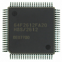
Manufacturer Part Number
HD64F2612FA20
Description
IC H8S MCU FLASH 128K 80QFP
Manufacturer
Renesas Electronics America
Series
H8® H8S/2600r
Specifications of HD64F2612FA20
Core Processor
H8S/2600
Core Size
16-Bit
Speed
20MHz
Connectivity
CAN, SCI
Peripherals
POR, PWM, WDT
Number Of I /o
43
Program Memory Size
128KB (128K x 8)
Program Memory Type
FLASH
Ram Size
4K x 8
Voltage - Supply (vcc/vdd)
4.5 V ~ 5.5 V
Data Converters
A/D 12x10b
Oscillator Type
Internal
Operating Temperature
-20°C ~ 75°C
Package / Case
80-QFP
Lead Free Status / RoHS Status
Contains lead / RoHS non-compliant
Eeprom Size
-
Available stocks
Company
Part Number
Manufacturer
Quantity
Price

Part Number:
HD64F2612FA20
Manufacturer:
RENESAS/瑞萨
Quantity:
20 000
Part Number:
HD64F2612FA20J
Manufacturer:
RENESAS/瑞萨
Quantity:
20 000


Table 10.14 TIOR_1 (channel 1) ................................................................................................ 176
Table 10.15 TIOR_2 (channel 2) ................................................................................................ 177
Table 10.16 TIORH_3 (channel 3).............................................................................................. 178
Table 10.17 TIORL_3 (channel 3) .............................................................................................. 179
Table 10.18 TIOR_4 (channel 4) ................................................................................................ 180
Table 10.19 TIOR_5 (channel 5) ................................................................................................ 181
Table 10.20 TIORH_0 (channel 0).............................................................................................. 182
Table 10.21 TIORL_0 (channel 0) .............................................................................................. 183
Table 10.22 TIOR_1 (channel 1) ................................................................................................ 184
Table 10.23 TIOR_2 (channel 2) ................................................................................................ 185
Table 10.24 TIORH_3 (channel 3).............................................................................................. 186
Table 10.25 TIORL_3 (channel 3) .............................................................................................. 187
Table 10.26 TIOR_4 (channel 4) ................................................................................................ 188
Table 10.27 TIOR_5 (channel 5) ................................................................................................ 189
Table 10.28 Register Combinations in Buffer Operation............................................................ 205
Table 10.29 Cascaded Combinations .......................................................................................... 209
Table 10.30 PWM Output Registers and Output Pins................................................................. 212
Table 10.31 Phase Counting Mode Clock Input Pins.................................................................. 216
Table 10.32 Up/Down-Count Conditions in Phase Counting Mode 1 ........................................ 218
Table 10.33 Up/Down-Count Conditions in Phase Counting Mode 2 ........................................ 219
Table 10.34 Up/Down-Count Conditions in Phase Counting Mode 3 ........................................ 220
Table 10.35 Up/Down-Count Conditions in Phase Counting Mode 4 ........................................ 221
Table 10.36 TPU Interrupts......................................................................................................... 224
Section 11 Motor Management Timer (MMT)
Table 11.1
Table 11.2
Table 11.3
Table 11.4
Section 12 Programmable Pulse Generator (PPG)
Table 12.1
Section 13 Watchdog Timer
Table 13.1
Section 14 Serial Communication Interface (SCI)
Table 14.1
Table 14.2
Table 14.3
Table 14.4
Pin Configuration .................................................................................................... 247
Initial Values of TBRU to TBRW and Initial Output.............................................. 259
MMT Interrupt Sources........................................................................................... 263
Pin Configuration .................................................................................................... 275
PPG I/O Pins ........................................................................................................... 283
WDT Interrupt Source............................................................................................. 309
Pin Configuration .................................................................................................... 315
Relationships between the N Setting in BRR and Bit Rate B ................................. 331
BRR Settings for Various Bit Rates (Asynchronous Mode) ................................... 332
Maximum Bit Rate for Each Frequency (Asynchronous Mode) ............................. 334
Rev. 7.00 Sep. 11, 2009 Page xxxi of xxxiv
REJ09B0211-0700
Related parts for HD64F2612FA20
Image
Part Number
Description
Manufacturer
Datasheet
Request
R


Part Number:
Description:
KIT STARTER FOR M16C/29
Manufacturer:
Renesas Electronics America
Datasheet:

Part Number:
Description:
KIT STARTER FOR R8C/2D
Manufacturer:
Renesas Electronics America
Datasheet:

Part Number:
Description:
R0K33062P STARTER KIT
Manufacturer:
Renesas Electronics America
Datasheet:

Part Number:
Description:
KIT STARTER FOR R8C/23 E8A
Manufacturer:
Renesas Electronics America
Datasheet:

Part Number:
Description:
KIT STARTER FOR R8C/25
Manufacturer:
Renesas Electronics America
Datasheet:

Part Number:
Description:
KIT STARTER H8S2456 SHARPE DSPLY
Manufacturer:
Renesas Electronics America
Datasheet:

Part Number:
Description:
KIT STARTER FOR R8C38C
Manufacturer:
Renesas Electronics America
Datasheet:

Part Number:
Description:
KIT STARTER FOR R8C35C
Manufacturer:
Renesas Electronics America
Datasheet:

Part Number:
Description:
KIT STARTER FOR R8CL3AC+LCD APPS
Manufacturer:
Renesas Electronics America
Datasheet:
Part Number:
Description:
KIT STARTER FOR RX610
Manufacturer:
Renesas Electronics America
Datasheet:

Part Number:
Description:
KIT STARTER FOR R32C/118
Manufacturer:
Renesas Electronics America
Datasheet:

Part Number:
Description:
KIT DEV RSK-R8C/26-29
Manufacturer:
Renesas Electronics America
Datasheet:

Part Number:
Description:
KIT STARTER FOR SH7124
Manufacturer:
Renesas Electronics America
Datasheet:

Part Number:
Description:
KIT STARTER FOR H8SX/1622
Manufacturer:
Renesas Electronics America
Datasheet: