HD64F2612FA20 Renesas Electronics America, HD64F2612FA20 Datasheet - Page 24
HD64F2612FA20
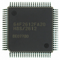
Manufacturer Part Number
HD64F2612FA20
Description
IC H8S MCU FLASH 128K 80QFP
Manufacturer
Renesas Electronics America
Series
H8® H8S/2600r
Specifications of HD64F2612FA20
Core Processor
H8S/2600
Core Size
16-Bit
Speed
20MHz
Connectivity
CAN, SCI
Peripherals
POR, PWM, WDT
Number Of I /o
43
Program Memory Size
128KB (128K x 8)
Program Memory Type
FLASH
Ram Size
4K x 8
Voltage - Supply (vcc/vdd)
4.5 V ~ 5.5 V
Data Converters
A/D 12x10b
Oscillator Type
Internal
Operating Temperature
-20°C ~ 75°C
Package / Case
80-QFP
Lead Free Status / RoHS Status
Contains lead / RoHS non-compliant
Eeprom Size
-
Available stocks
Company
Part Number
Manufacturer
Quantity
Price

Part Number:
HD64F2612FA20
Manufacturer:
RENESAS/瑞萨
Quantity:
20 000
Part Number:
HD64F2612FA20J
Manufacturer:
RENESAS/瑞萨
Quantity:
20 000


Section 1 Overview
Figure 1.1
Figure 1.2
Figure 1.3
Figure 1.4
Section 2 CPU
Figure 2.1
Figure 2.2
Figure 2.3
Figure 2.4
Figure 2.5
Figure 2.6
Figure 2.7
Figure 2.8
Figure 2.9
Figure 2.9
Figure 2.10 Memory Data Formats............................................................................................... 29
Figure 2.11 Instruction Formats (Examples) ................................................................................ 41
Figure 2.12 Branch Address Specification in Memory Indirect Mode......................................... 45
Figure 2.13 State Transitions........................................................................................................ 49
Section 3 MCU Operating Modes
Figure 3.1
Section 4 Exception Handling
Figure 4.1
Figure 4.2
Figure 4.3
Figure 4.4
Section 5 Interrupt Controller
Figure 5.1
Figure 5.2
Figure 5.3
Figure 5.4
Figure 5.5
Figure 5.6
Rev. 7.00 Sep. 11, 2009 Page xxii of xxxiv
REJ09B0211-0700
Internal Block Diagram (HD64F2612, HD6432612, and HD6432611)...................... 3
Internal Block Diagram (HD6432616 and HD6432614) ............................................ 4
Pin Arrangement (HD64F2612, HD6432612, and HD6432611) ................................ 5
Pin Arrangement (HD6432616 and HD6432614)....................................................... 6
Exception Vector Table (Normal Mode)................................................................... 17
Stack Structure in Normal Mode............................................................................... 17
Exception Vector Table (Advanced Mode)............................................................... 18
Stack Structure in Advanced Mode........................................................................... 19
Memory Map............................................................................................................. 20
CPU Registers ........................................................................................................... 21
Usage of General Registers ....................................................................................... 22
Stack.......................................................................................................................... 23
General Register Data Formats (1)............................................................................ 27
General Register Data Formats (2)............................................................................ 28
Address Map (H8S/2612, H8S/2611, H8S/2616, H8S/2614) ................................... 55
Reset Sequence (Advanced Mode with On-Chip ROM Enabled)............................. 60
Reset Sequence
(Advanced Mode with On-Chip ROM Disabled: Cannot be Used in this LSI) ........ 61
Stack Status after Exception Handling ...................................................................... 64
Operation when SP Value is Odd.............................................................................. 65
Block Diagram of Interrupt Controller...................................................................... 68
Block Diagram of Interrupts IRQ0 to IRQ5 .............................................................. 75
Flowchart of Procedure Up to Interrupt Acceptance in Interrupt Control Mode 0... 80
Flowchart of Procedure Up to Interrupt Acceptance in Control Mode 2 .................. 82
Interrupt Exception Handling .................................................................................... 84
Contention between Interrupt Generation and Disabling .......................................... 87
Figures
Related parts for HD64F2612FA20
Image
Part Number
Description
Manufacturer
Datasheet
Request
R


Part Number:
Description:
KIT STARTER FOR M16C/29
Manufacturer:
Renesas Electronics America
Datasheet:

Part Number:
Description:
KIT STARTER FOR R8C/2D
Manufacturer:
Renesas Electronics America
Datasheet:

Part Number:
Description:
R0K33062P STARTER KIT
Manufacturer:
Renesas Electronics America
Datasheet:

Part Number:
Description:
KIT STARTER FOR R8C/23 E8A
Manufacturer:
Renesas Electronics America
Datasheet:

Part Number:
Description:
KIT STARTER FOR R8C/25
Manufacturer:
Renesas Electronics America
Datasheet:

Part Number:
Description:
KIT STARTER H8S2456 SHARPE DSPLY
Manufacturer:
Renesas Electronics America
Datasheet:

Part Number:
Description:
KIT STARTER FOR R8C38C
Manufacturer:
Renesas Electronics America
Datasheet:

Part Number:
Description:
KIT STARTER FOR R8C35C
Manufacturer:
Renesas Electronics America
Datasheet:

Part Number:
Description:
KIT STARTER FOR R8CL3AC+LCD APPS
Manufacturer:
Renesas Electronics America
Datasheet:
Part Number:
Description:
KIT STARTER FOR RX610
Manufacturer:
Renesas Electronics America
Datasheet:

Part Number:
Description:
KIT STARTER FOR R32C/118
Manufacturer:
Renesas Electronics America
Datasheet:

Part Number:
Description:
KIT DEV RSK-R8C/26-29
Manufacturer:
Renesas Electronics America
Datasheet:

Part Number:
Description:
KIT STARTER FOR SH7124
Manufacturer:
Renesas Electronics America
Datasheet:

Part Number:
Description:
KIT STARTER FOR H8SX/1622
Manufacturer:
Renesas Electronics America
Datasheet: