HD64F2612FA20 Renesas Electronics America, HD64F2612FA20 Datasheet - Page 29
HD64F2612FA20
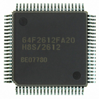
Manufacturer Part Number
HD64F2612FA20
Description
IC H8S MCU FLASH 128K 80QFP
Manufacturer
Renesas Electronics America
Series
H8® H8S/2600r
Specifications of HD64F2612FA20
Core Processor
H8S/2600
Core Size
16-Bit
Speed
20MHz
Connectivity
CAN, SCI
Peripherals
POR, PWM, WDT
Number Of I /o
43
Program Memory Size
128KB (128K x 8)
Program Memory Type
FLASH
Ram Size
4K x 8
Voltage - Supply (vcc/vdd)
4.5 V ~ 5.5 V
Data Converters
A/D 12x10b
Oscillator Type
Internal
Operating Temperature
-20°C ~ 75°C
Package / Case
80-QFP
Lead Free Status / RoHS Status
Contains lead / RoHS non-compliant
Eeprom Size
-
Available stocks
Company
Part Number
Manufacturer
Quantity
Price

Part Number:
HD64F2612FA20
Manufacturer:
RENESAS/瑞萨
Quantity:
20 000
Part Number:
HD64F2612FA20J
Manufacturer:
RENESAS/瑞萨
Quantity:
20 000


Figure 14.34 Sample Flowchart for Mode Transition during Transmission................................ 379
Figure 14.35 Pin States during Transmission in Asynchronous Mode (Internal Clock) ............. 379
Figure 14.36 Pin States during Transmission in Clocked Synchronous Mode
Figure 14.37 Sample Flowchart for Mode Transition during Reception ..................................... 381
Figure 14.38 Operation when Switching from SCK Pin to Port Pin ........................................... 382
Section 15 Controller Area Network (HCAN)
Figure 15.1
Figure 15.2
Figure 15.3
Figure 15.4
Figure 15.5
Figure 15.6
Figure 15.7
Figure 15.8
Figure 15.9
Figure 15.10 Transmit Message Cancellation Flowchart ............................................................ 420
Figure 15.11 Reception Flowchart .............................................................................................. 421
Figure 15.12 Unread Message Overwrite Flowchart................................................................... 424
Figure 15.13 HCAN Sleep Mode Flowchart ............................................................................... 425
Figure 15.14 HCAN Halt Mode Flowchart ................................................................................. 427
Figure 15.15 DTC Transfer Flowchart ........................................................................................ 429
Figure 15.16 High-Speed Interface Using PCA82C250.............................................................. 430
Section 16 A/D Converter
Figure 16.1
Figure 16.2
Figure 16.3
Figure 16.4
Figure 16.5
Figure 16.6
Figure 16.7
Figure 16.8
Section 18 ROM
Figure 18.1
Figure 18.2
Figure 18.3
Figure 18.4
Figure 18.5
(Internal Clock) ...................................................................................................... 380
HCAN Block Diagram ........................................................................................... 384
Message Control Register Configuration ............................................................... 409
Standard Format ..................................................................................................... 409
Extended Format .................................................................................................... 409
Message Data Configuration .................................................................................. 411
Hardware Reset Flowchart ..................................................................................... 413
Software Reset Flowchart ...................................................................................... 414
Detailed Description of One Bit ............................................................................. 415
Transmission Flowchart ......................................................................................... 418
Block Diagram of A/D Converter .......................................................................... 436
A/D Conversion Timing......................................................................................... 443
External Trigger Input Timing ............................................................................... 445
A/D Conversion Precision Definitions................................................................... 447
A/D Conversion Precision Definitions................................................................... 447
Example of Analog Input Circuit ........................................................................... 448
Example of Analog Input Protection Circuit.......................................................... 450
Analog Input Pin Equivalent Circuit ...................................................................... 450
Block Diagram of Flash Memory........................................................................... 454
Flash Memory State Transitions............................................................................. 455
Boot Mode.............................................................................................................. 456
User Program Mode ............................................................................................... 457
Flash Memory Block Configuration....................................................................... 458
Rev. 7.00 Sep. 11, 2009 Page xxvii of xxxiv
REJ09B0211-0700
Related parts for HD64F2612FA20
Image
Part Number
Description
Manufacturer
Datasheet
Request
R


Part Number:
Description:
KIT STARTER FOR M16C/29
Manufacturer:
Renesas Electronics America
Datasheet:

Part Number:
Description:
KIT STARTER FOR R8C/2D
Manufacturer:
Renesas Electronics America
Datasheet:

Part Number:
Description:
R0K33062P STARTER KIT
Manufacturer:
Renesas Electronics America
Datasheet:

Part Number:
Description:
KIT STARTER FOR R8C/23 E8A
Manufacturer:
Renesas Electronics America
Datasheet:

Part Number:
Description:
KIT STARTER FOR R8C/25
Manufacturer:
Renesas Electronics America
Datasheet:

Part Number:
Description:
KIT STARTER H8S2456 SHARPE DSPLY
Manufacturer:
Renesas Electronics America
Datasheet:

Part Number:
Description:
KIT STARTER FOR R8C38C
Manufacturer:
Renesas Electronics America
Datasheet:

Part Number:
Description:
KIT STARTER FOR R8C35C
Manufacturer:
Renesas Electronics America
Datasheet:

Part Number:
Description:
KIT STARTER FOR R8CL3AC+LCD APPS
Manufacturer:
Renesas Electronics America
Datasheet:
Part Number:
Description:
KIT STARTER FOR RX610
Manufacturer:
Renesas Electronics America
Datasheet:

Part Number:
Description:
KIT STARTER FOR R32C/118
Manufacturer:
Renesas Electronics America
Datasheet:

Part Number:
Description:
KIT DEV RSK-R8C/26-29
Manufacturer:
Renesas Electronics America
Datasheet:

Part Number:
Description:
KIT STARTER FOR SH7124
Manufacturer:
Renesas Electronics America
Datasheet:

Part Number:
Description:
KIT STARTER FOR H8SX/1622
Manufacturer:
Renesas Electronics America
Datasheet: