HD64F2612FA20 Renesas Electronics America, HD64F2612FA20 Datasheet - Page 404
HD64F2612FA20
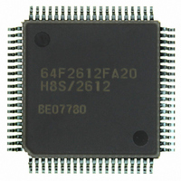
Manufacturer Part Number
HD64F2612FA20
Description
IC H8S MCU FLASH 128K 80QFP
Manufacturer
Renesas Electronics America
Series
H8® H8S/2600r
Specifications of HD64F2612FA20
Core Processor
H8S/2600
Core Size
16-Bit
Speed
20MHz
Connectivity
CAN, SCI
Peripherals
POR, PWM, WDT
Number Of I /o
43
Program Memory Size
128KB (128K x 8)
Program Memory Type
FLASH
Ram Size
4K x 8
Voltage - Supply (vcc/vdd)
4.5 V ~ 5.5 V
Data Converters
A/D 12x10b
Oscillator Type
Internal
Operating Temperature
-20°C ~ 75°C
Package / Case
80-QFP
Lead Free Status / RoHS Status
Contains lead / RoHS non-compliant
Eeprom Size
-
Available stocks
Company
Part Number
Manufacturer
Quantity
Price

Part Number:
HD64F2612FA20
Manufacturer:
RENESAS/瑞萨
Quantity:
20 000
Part Number:
HD64F2612FA20J
Manufacturer:
RENESAS/瑞萨
Quantity:
20 000


Section 14 Serial Communication Interface (SCI)
14.7.5
Before transmitting and receiving data, initialize the SCI as described below. Initialization is also
necessary when switching from transmit mode to receive mode, or vice versa.
1. Clear the TE and RE bits in SCR to 0.
2. Clear the error flags ERS, PER, and ORER in SSR to 0.
3. Set the GM, BLK, O/E, BCP0, BCP1, CKS0, CKS1 bits in SMR. Set the PE bit to 1.
4. Set the SMIF, SDIR, and SINV bits in SCMR.
5. Set the value corresponding to the bit rate in BRR.
6. Set the CKE0 and CKE1 bits in SCR. Clear the TIE, RIE, TE, RE, MPIE, and TEIE bits to 0.
7. Wait at least one bit interval, then set the TIE, RIE, TE, and RE bits in SCR. Do not set the TE
To switch from receive mode to transmit mode, after checking that the SCI has finished reception,
initialize the SCI, and set RE to 0 and TE to 1. Whether SCI has finished reception or not can be
checked with the RDRF, PER, or ORER flags. To switch from transmit mode to receive mode,
Rev. 7.00 Sep. 11, 2009 Page 368 of 566
REJ09B0211-0700
When the SMIF bit is set to 1, the TxD and RxD pins are both switched from ports to SCI pins,
and are placed in the high-impedance state.
If the CKE0 bit is set to 1, the clock is output from the SCK pin.
bit and RE bit at the same time, except for self-diagnosis.
Internal
basic clock
Receive data
(RxD)
Synchronization
sampling timing
Data sampling
timing
Initialization
Figure 14.25 Receive Data Sampling Timing in Smart Card Mode
186 clocks
0
(Using Clock of 372 Times the Transfer Rate)
185
372 clocks
Start bit
371
0
D0
185
371 0
D1
Related parts for HD64F2612FA20
Image
Part Number
Description
Manufacturer
Datasheet
Request
R


Part Number:
Description:
KIT STARTER FOR M16C/29
Manufacturer:
Renesas Electronics America
Datasheet:

Part Number:
Description:
KIT STARTER FOR R8C/2D
Manufacturer:
Renesas Electronics America
Datasheet:

Part Number:
Description:
R0K33062P STARTER KIT
Manufacturer:
Renesas Electronics America
Datasheet:

Part Number:
Description:
KIT STARTER FOR R8C/23 E8A
Manufacturer:
Renesas Electronics America
Datasheet:

Part Number:
Description:
KIT STARTER FOR R8C/25
Manufacturer:
Renesas Electronics America
Datasheet:

Part Number:
Description:
KIT STARTER H8S2456 SHARPE DSPLY
Manufacturer:
Renesas Electronics America
Datasheet:

Part Number:
Description:
KIT STARTER FOR R8C38C
Manufacturer:
Renesas Electronics America
Datasheet:

Part Number:
Description:
KIT STARTER FOR R8C35C
Manufacturer:
Renesas Electronics America
Datasheet:

Part Number:
Description:
KIT STARTER FOR R8CL3AC+LCD APPS
Manufacturer:
Renesas Electronics America
Datasheet:
Part Number:
Description:
KIT STARTER FOR RX610
Manufacturer:
Renesas Electronics America
Datasheet:

Part Number:
Description:
KIT STARTER FOR R32C/118
Manufacturer:
Renesas Electronics America
Datasheet:

Part Number:
Description:
KIT DEV RSK-R8C/26-29
Manufacturer:
Renesas Electronics America
Datasheet:

Part Number:
Description:
KIT STARTER FOR SH7124
Manufacturer:
Renesas Electronics America
Datasheet:

Part Number:
Description:
KIT STARTER FOR H8SX/1622
Manufacturer:
Renesas Electronics America
Datasheet: