HD64F2612FA20 Renesas Electronics America, HD64F2612FA20 Datasheet - Page 414
HD64F2612FA20
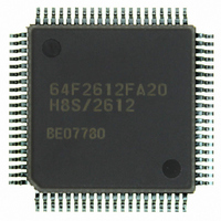
Manufacturer Part Number
HD64F2612FA20
Description
IC H8S MCU FLASH 128K 80QFP
Manufacturer
Renesas Electronics America
Series
H8® H8S/2600r
Specifications of HD64F2612FA20
Core Processor
H8S/2600
Core Size
16-Bit
Speed
20MHz
Connectivity
CAN, SCI
Peripherals
POR, PWM, WDT
Number Of I /o
43
Program Memory Size
128KB (128K x 8)
Program Memory Type
FLASH
Ram Size
4K x 8
Voltage - Supply (vcc/vdd)
4.5 V ~ 5.5 V
Data Converters
A/D 12x10b
Oscillator Type
Internal
Operating Temperature
-20°C ~ 75°C
Package / Case
80-QFP
Lead Free Status / RoHS Status
Contains lead / RoHS non-compliant
Eeprom Size
-
Available stocks
Company
Part Number
Manufacturer
Quantity
Price

Part Number:
HD64F2612FA20
Manufacturer:
RENESAS/瑞萨
Quantity:
20 000
Part Number:
HD64F2612FA20J
Manufacturer:
RENESAS/瑞萨
Quantity:
20 000


Section 14 Serial Communication Interface (SCI)
14.9.5
When the external clock source is used as a synchronization clock, update TDR by the DTC and
wait for at least five φ clock cycles before allowing the transmit clock to be input. If the transmit
clock is input within four clock cycles after TDR modification, the SCI may malfunction (figure
14.33).
When using the DTC to read RDR, be sure to set the receive end interrupt source (RXI) as a DTC
activation source.
14.9.6
Transmission: Before making the transition to module stop, software standby, watch, sub-active,
or sub-sleep mode, stop all transmit operations (TE = TIE = TEIE = 0). TSR, TDR, and SSR are
reset. The states of the output pins during each mode depend on the port settings, and the pins
output a high-level signal after mode is cancelled and then the TE is set to 1 again. If the transition
is made during data transmission, the data being transmitted will be undefined.
To transmit data in the same transmission mode after mode cancellation, set TE to 1, read SSR,
write to TDR, clear TDRE in this order, and then start transmission. To transmit data in a different
transmission mode, initialize the SCI first.
Figure 14.34 shows a sample flowchart for mode transition during transmission. Figures 14.35 and
14.36 show the pin states during transmission.
Before making the transition from the transmission mode using DTC transfer to module stop,
software standby, watch, sub-active, or sub-sleep mode, stop all transmit operations (TE = TIE =
TEIE = 0). Setting TE and TIE to 1 after mode cancellation generates a TXI interrupt request to
start transmission using the DTC.
Rev. 7.00 Sep. 11, 2009 Page 378 of 566
REJ09B0211-0700
Figure 14.33 Sample Transmission using DTC in Clocked Synchronous Mode
Restrictions on Using DTC
SCI Operations during Mode Transitions
SCK
TDRE
Serial data
Note: When external clock is supplied, t must be more than four clock cycles.
t
LSB
D0
D1
D2
D3
D4
D5
D6
D7
Related parts for HD64F2612FA20
Image
Part Number
Description
Manufacturer
Datasheet
Request
R


Part Number:
Description:
KIT STARTER FOR M16C/29
Manufacturer:
Renesas Electronics America
Datasheet:

Part Number:
Description:
KIT STARTER FOR R8C/2D
Manufacturer:
Renesas Electronics America
Datasheet:

Part Number:
Description:
R0K33062P STARTER KIT
Manufacturer:
Renesas Electronics America
Datasheet:

Part Number:
Description:
KIT STARTER FOR R8C/23 E8A
Manufacturer:
Renesas Electronics America
Datasheet:

Part Number:
Description:
KIT STARTER FOR R8C/25
Manufacturer:
Renesas Electronics America
Datasheet:

Part Number:
Description:
KIT STARTER H8S2456 SHARPE DSPLY
Manufacturer:
Renesas Electronics America
Datasheet:

Part Number:
Description:
KIT STARTER FOR R8C38C
Manufacturer:
Renesas Electronics America
Datasheet:

Part Number:
Description:
KIT STARTER FOR R8C35C
Manufacturer:
Renesas Electronics America
Datasheet:

Part Number:
Description:
KIT STARTER FOR R8CL3AC+LCD APPS
Manufacturer:
Renesas Electronics America
Datasheet:
Part Number:
Description:
KIT STARTER FOR RX610
Manufacturer:
Renesas Electronics America
Datasheet:

Part Number:
Description:
KIT STARTER FOR R32C/118
Manufacturer:
Renesas Electronics America
Datasheet:

Part Number:
Description:
KIT DEV RSK-R8C/26-29
Manufacturer:
Renesas Electronics America
Datasheet:

Part Number:
Description:
KIT STARTER FOR SH7124
Manufacturer:
Renesas Electronics America
Datasheet:

Part Number:
Description:
KIT STARTER FOR H8SX/1622
Manufacturer:
Renesas Electronics America
Datasheet: