HD64F2612FA20 Renesas Electronics America, HD64F2612FA20 Datasheet - Page 21
HD64F2612FA20
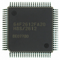
Manufacturer Part Number
HD64F2612FA20
Description
IC H8S MCU FLASH 128K 80QFP
Manufacturer
Renesas Electronics America
Series
H8® H8S/2600r
Specifications of HD64F2612FA20
Core Processor
H8S/2600
Core Size
16-Bit
Speed
20MHz
Connectivity
CAN, SCI
Peripherals
POR, PWM, WDT
Number Of I /o
43
Program Memory Size
128KB (128K x 8)
Program Memory Type
FLASH
Ram Size
4K x 8
Voltage - Supply (vcc/vdd)
4.5 V ~ 5.5 V
Data Converters
A/D 12x10b
Oscillator Type
Internal
Operating Temperature
-20°C ~ 75°C
Package / Case
80-QFP
Lead Free Status / RoHS Status
Contains lead / RoHS non-compliant
Eeprom Size
-
Available stocks
Company
Part Number
Manufacturer
Quantity
Price

Part Number:
HD64F2612FA20
Manufacturer:
RENESAS/瑞萨
Quantity:
20 000
Part Number:
HD64F2612FA20J
Manufacturer:
RENESAS/瑞萨
Quantity:
20 000


Section 16 A/D Converter..................................................................................435
16.1 Features .............................................................................................................................. 435
16.2 Input/Output Pins ............................................................................................................... 437
16.3 Register Description........................................................................................................... 438
16.4 Operation............................................................................................................................ 442
16.5 Interrupts ............................................................................................................................ 445
16.6 A/D Conversion Precision Definitions............................................................................... 446
16.7 Usage Notes ....................................................................................................................... 448
Section 17 RAM ................................................................................................451
Section 18 ROM ................................................................................................453
18.1 Features .............................................................................................................................. 453
18.2 Mode Transitions ............................................................................................................... 454
18.3 Block Configuration........................................................................................................... 458
18.4 Input/Output Pins ............................................................................................................... 459
18.5 Register Descriptions ......................................................................................................... 459
15.8.5 Error Counters....................................................................................................... 431
15.8.6 Register Access..................................................................................................... 431
15.8.7 HCAN Medium-Speed Mode ............................................................................... 431
15.8.8 Register Hold in Standby Modes .......................................................................... 431
15.8.9 Usage of Bit Manipulation Instructions ................................................................ 431
15.8.10 HCAN TXCR Operation....................................................................................... 432
15.8.11 HCAN Transmit Procedure................................................................................... 433
15.8.12 Note on Releasing the HCAN Reset or HCAN Sleep........................................... 433
15.8.13 Note on Accessing Mailbox during the HCAN Sleep........................................... 433
16.3.1 A/D Data Registers A to D (ADDRA to ADDRD) .............................................. 438
16.3.2 A/D Control/Status Register (ADCSR) ................................................................ 439
16.3.3 A/D Control Register (ADCR) ............................................................................. 441
16.4.1 Single Mode.......................................................................................................... 442
16.4.2 Scan Mode ............................................................................................................ 442
16.4.3 Input Sampling and A/D Conversion Time........................................................... 443
16.4.4 External Trigger Input Timing.............................................................................. 445
16.7.1 Module Stop Mode Setting ................................................................................... 448
16.7.2 Permissible Signal Source Impedance .................................................................. 448
16.7.3 Influences on Absolute Precision.......................................................................... 448
16.7.4 Range of Analog Power Supply and Other Pin Settings ....................................... 449
16.7.5 Notes on Board Design ......................................................................................... 449
16.7.6 Notes on Noise Countermeasures ......................................................................... 449
18.5.1 Flash Memory Control Register 1 (FLMCR1)...................................................... 459
Rev. 7.00 Sep. 11, 2009 Page xix of xxxiv
REJ09B0211-0700
Related parts for HD64F2612FA20
Image
Part Number
Description
Manufacturer
Datasheet
Request
R


Part Number:
Description:
KIT STARTER FOR M16C/29
Manufacturer:
Renesas Electronics America
Datasheet:

Part Number:
Description:
KIT STARTER FOR R8C/2D
Manufacturer:
Renesas Electronics America
Datasheet:

Part Number:
Description:
R0K33062P STARTER KIT
Manufacturer:
Renesas Electronics America
Datasheet:

Part Number:
Description:
KIT STARTER FOR R8C/23 E8A
Manufacturer:
Renesas Electronics America
Datasheet:

Part Number:
Description:
KIT STARTER FOR R8C/25
Manufacturer:
Renesas Electronics America
Datasheet:

Part Number:
Description:
KIT STARTER H8S2456 SHARPE DSPLY
Manufacturer:
Renesas Electronics America
Datasheet:

Part Number:
Description:
KIT STARTER FOR R8C38C
Manufacturer:
Renesas Electronics America
Datasheet:

Part Number:
Description:
KIT STARTER FOR R8C35C
Manufacturer:
Renesas Electronics America
Datasheet:

Part Number:
Description:
KIT STARTER FOR R8CL3AC+LCD APPS
Manufacturer:
Renesas Electronics America
Datasheet:
Part Number:
Description:
KIT STARTER FOR RX610
Manufacturer:
Renesas Electronics America
Datasheet:

Part Number:
Description:
KIT STARTER FOR R32C/118
Manufacturer:
Renesas Electronics America
Datasheet:

Part Number:
Description:
KIT DEV RSK-R8C/26-29
Manufacturer:
Renesas Electronics America
Datasheet:

Part Number:
Description:
KIT STARTER FOR SH7124
Manufacturer:
Renesas Electronics America
Datasheet:

Part Number:
Description:
KIT STARTER FOR H8SX/1622
Manufacturer:
Renesas Electronics America
Datasheet: