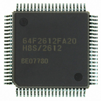
HD64F2612FA20 Renesas Electronics America, HD64F2612FA20 Datasheet - Page 499

HD64F2612FA20
Manufacturer Part Number
HD64F2612FA20
Description
IC H8S MCU FLASH 128K 80QFP
Manufacturer
Renesas Electronics America
Series
H8® H8S/2600r
Specifications of HD64F2612FA20
Core Processor
H8S/2600
Core Size
16-Bit
Speed
20MHz
Connectivity
CAN, SCI
Peripherals
POR, PWM, WDT
Number Of I /o
43
Program Memory Size
128KB (128K x 8)
Program Memory Type
FLASH
Ram Size
4K x 8
Voltage - Supply (vcc/vdd)
4.5 V ~ 5.5 V
Data Converters
A/D 12x10b
Oscillator Type
Internal
Operating Temperature
-20°C ~ 75°C
Package / Case
80-QFP
Lead Free Status / RoHS Status
Contains lead / RoHS non-compliant
Eeprom Size
-
Available stocks
Company
Part Number
Manufacturer
Quantity
Price
Part Number:
HD64F2612FA20
Manufacturer:
RENESAS/瑞萨
Quantity:
20 000
Part Number:
HD64F2612FA20J
Manufacturer:
RENESAS/瑞萨
Quantity:
20 000
- Current page: 499 of 606
- Download datasheet (4Mb)
Bit
2
1
0
18.6
There are two modes for programming/erasing of the flash memory; boot mode, which enables on-
board programming/erasing, and programmer mode, in which programming/erasing is performed
with a PROM programmer. On-board programming/erasing can also be performed in user
program mode. At reset-start in reset mode, this LSI changes to a mode depending on the MD pin
settings and FWE pin setting, as shown in table 18.3. The input level of each pin must be defined
four states before the reset ends.
When changing to boot mode, the boot program built into this LSI is initiated. The boot program
transfers the programming control program from the externally-connected host to on-chip RAM
via SCI_2. After erasing the entire flash memory, the programming control program is executed.
This can be used for programming initial values in the on-board state or for a forcible return when
programming/erasing can no longer be done in user program mode. In user program mode,
individual blocks can be erased and programmed by branching to the user program/erase control
program prepared by the user.
Table 18.3 Setting On-Board Programming Modes
MD2
1
0
Bit Name
RAM2
RAM1
RAM0
On-Board Programming Modes
MD1
1
1
MD0
1
1
Initial Value
0
0
0
FWE
1
1
R/W
R/W
R/W
R/W
LSI State after Reset End
User Mode
Boot Mode
Description
Flash Memory Area Selection
When the RAMS bit is set to 1, one of the following
flash memory areas are selected to overlap the
RAM area of H'FFE000 to H'FFE3FF. The areas
correspond with 1-kbyte erase blocks.
00X: H'000000 to H'0003FF (EB0)
01X: H'000400 to H'0007FF (EB1)
10X: H'000800 to H'000BFF (EB2)
11X: H'000C00 to H'000FFF (EB3)
Note: X: Don’t care
Rev. 7.00 Sep. 11, 2009 Page 463 of 566
REJ09B0211-0700
Section 18 ROM
Related parts for HD64F2612FA20
Image
Part Number
Description
Manufacturer
Datasheet
Request
R

Part Number:
Description:
KIT STARTER FOR M16C/29
Manufacturer:
Renesas Electronics America
Datasheet:

Part Number:
Description:
KIT STARTER FOR R8C/2D
Manufacturer:
Renesas Electronics America
Datasheet:

Part Number:
Description:
R0K33062P STARTER KIT
Manufacturer:
Renesas Electronics America
Datasheet:

Part Number:
Description:
KIT STARTER FOR R8C/23 E8A
Manufacturer:
Renesas Electronics America
Datasheet:

Part Number:
Description:
KIT STARTER FOR R8C/25
Manufacturer:
Renesas Electronics America
Datasheet:

Part Number:
Description:
KIT STARTER H8S2456 SHARPE DSPLY
Manufacturer:
Renesas Electronics America
Datasheet:

Part Number:
Description:
KIT STARTER FOR R8C38C
Manufacturer:
Renesas Electronics America
Datasheet:

Part Number:
Description:
KIT STARTER FOR R8C35C
Manufacturer:
Renesas Electronics America
Datasheet:

Part Number:
Description:
KIT STARTER FOR R8CL3AC+LCD APPS
Manufacturer:
Renesas Electronics America
Datasheet:

Part Number:
Description:
KIT STARTER FOR RX610
Manufacturer:
Renesas Electronics America
Datasheet:

Part Number:
Description:
KIT STARTER FOR R32C/118
Manufacturer:
Renesas Electronics America
Datasheet:

Part Number:
Description:
KIT DEV RSK-R8C/26-29
Manufacturer:
Renesas Electronics America
Datasheet:

Part Number:
Description:
KIT STARTER FOR SH7124
Manufacturer:
Renesas Electronics America
Datasheet:

Part Number:
Description:
KIT STARTER FOR H8SX/1622
Manufacturer:
Renesas Electronics America
Datasheet:


