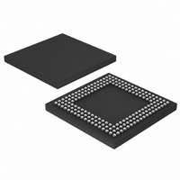
LPC2458FET180,551 NXP Semiconductors, LPC2458FET180,551 Datasheet - Page 332

LPC2458FET180,551
Manufacturer Part Number
LPC2458FET180,551
Description
IC ARM7 MCU FLASH 512K 180TFBGA
Manufacturer
NXP Semiconductors
Series
LPC2400r
Specifications of LPC2458FET180,551
Core Processor
ARM7
Core Size
16/32-Bit
Speed
72MHz
Connectivity
CAN, EBI/EMI, Ethernet, I²C, Microwire, MMC, SPI, SSI, SSP, UART/USART, USB OTG
Peripherals
Brown-out Detect/Reset, DMA, I²S, POR, PWM, WDT
Number Of I /o
136
Program Memory Size
512KB (512K x 8)
Program Memory Type
FLASH
Ram Size
98K x 8
Voltage - Supply (vcc/vdd)
3 V ~ 3.6 V
Data Converters
A/D 8x10b; D/A 1x10b
Oscillator Type
Internal
Operating Temperature
-40°C ~ 85°C
Package / Case
180-TFBGA
Processor Series
LPC24
Core
ARM7TDMI-S
Data Bus Width
32 bit
Data Ram Size
98 KB
Interface Type
CAN, Ethernet, I2C, I2S, IrDA, SPI, SSP, UART, USB
Maximum Clock Frequency
72 MHz
Number Of Programmable I/os
136
Number Of Timers
4
Operating Supply Voltage
3.3 V
Maximum Operating Temperature
+ 85 C
Mounting Style
SMD/SMT
3rd Party Development Tools
MDK-ARM, RL-ARM, ULINK2, SAB-TFBGA180
Minimum Operating Temperature
- 40 C
On-chip Adc
10 bit, 8 Channel
On-chip Dac
10 bit, 1 Channel
Package
180TFBGA
Device Core
ARM7TDMI-S
Family Name
LPC2000
Maximum Speed
72 MHz
For Use With
622-1023 - BOARD SCKT ADAPTER FOR TFBGA180622-1005 - USB IN-CIRCUIT PROG ARM7 LPC2K
Lead Free Status / RoHS Status
Lead free / RoHS Compliant
Eeprom Size
-
Lead Free Status / Rohs Status
Details
Other names
568-4258
935282454551
LPC2458FET180-S
935282454551
LPC2458FET180-S
Available stocks
Company
Part Number
Manufacturer
Quantity
Price
Company:
Part Number:
LPC2458FET180,551
Manufacturer:
MICROCHIP
Quantity:
1 103
Company:
Part Number:
LPC2458FET180,551
Manufacturer:
NXP Semiconductors
Quantity:
10 000
- Current page: 332 of 792
- Download datasheet (5Mb)
NXP Semiconductors
UM10237_4
User manual
Fig 45. USB device controller block diagram
DMA interface
(AHB master)
(AHB slave)
interface
register
5.1 Analog transceiver
5.2 Serial Interface Engine (SIE)
5.3 Endpoint RAM (EP_RAM)
5.4 EP_RAM access control
The USB Device Controller has a built-in analog transceiver (ATX). The USB ATX
sends/receives the bi-directional D+ and D- signals of the USB bus.
The SIE implements the full USB protocol layer. It is completely hardwired for speed and
needs no firmware intervention. It handles transfer of data between the endpoint buffers in
EP_RAM and the USB bus. The functions of this block include: synchronization pattern
recognition, parallel/serial conversion, bit stuffing/de-stuffing, CRC checking/generation,
PID verification/generation, address recognition, and handshake evaluation/generation.
Each endpoint buffer is implemented as an SRAM based FIFO. The SRAM dedicated for
this purpose is called the EP_RAM. Each realized endpoint has a reserved space in the
EP_RAM. The total EP_RAM space required depends on the number of realized
endpoints, the maximum packet size of the endpoint, and whether the endpoint supports
double buffering.
The EP_RAM Access Control logic handles transfer of data from/to the EP_RAM and the
three sources that can access it: the CPU (via the Register Interface), the SIE, and the
DMA Engine.
USB DEVICE
BLOCK
INTERFACE
MASTER
INTERFACE
REGISTER
BUS
Rev. 04 — 26 August 2009
CONTROL
EP_RAM
ACCESS
EP_RAM
ENGINE
DMA
(4K)
Chapter 13: LPC24XX USB device controller
INTERFACE
ENGINE
SERIAL
UM10237
© NXP B.V. 2009. All rights reserved.
USB_CONNECT1,
USB_CONNECT2
USB_UP_LED1,
USB_UP_LED2
USB_D+1,
USB_D+2
USB_D-1,
USB_D-2
V
BUS
332 of 792
Related parts for LPC2458FET180,551
Image
Part Number
Description
Manufacturer
Datasheet
Request
R

Part Number:
Description:
NXP Semiconductors designed the LPC2458 microcontroller around a 16-bit/32-bitARM7TDMI-S CPU core with real-time debug interfaces that include both JTAG andembedded trace
Manufacturer:
NXP Semiconductors
Datasheet:
Part Number:
Description:
NXP Semiconductors designed the LPC2420/2460 microcontroller around a 16-bit/32-bitARM7TDMI-S CPU core with real-time debug interfaces that include both JTAG andembedded trace
Manufacturer:
NXP Semiconductors
Datasheet:
Part Number:
Description:
NXP Semiconductors designed the LPC2468 microcontroller around a 16-bit/32-bitARM7TDMI-S CPU core with real-time debug interfaces that include both JTAG andembedded trace
Manufacturer:
NXP Semiconductors
Datasheet:
Part Number:
Description:
NXP Semiconductors designed the LPC2470 microcontroller, powered by theARM7TDMI-S core, to be a highly integrated microcontroller for a wide range ofapplications that require advanced communications and high quality graphic displays
Manufacturer:
NXP Semiconductors
Datasheet:
Part Number:
Description:
NXP Semiconductors designed the LPC2478 microcontroller, powered by theARM7TDMI-S core, to be a highly integrated microcontroller for a wide range ofapplications that require advanced communications and high quality graphic displays
Manufacturer:
NXP Semiconductors
Datasheet:
Part Number:
Description:
The Philips Semiconductors XA (eXtended Architecture) family of 16-bit single-chip microcontrollers is powerful enough to easily handle the requirements of high performance embedded applications, yet inexpensive enough to compete in the market for hi
Manufacturer:
NXP Semiconductors
Datasheet:
Part Number:
Description:
The XA-S3 device is a member of Philips Semiconductors? XA(eXtended Architecture) family of high performance 16-bitsingle-chip microcontrollers
Manufacturer:
NXP Semiconductors
Datasheet:

Part Number:
Description:
The NXP BlueStreak LH75401/LH75411 family consists of two low-cost 16/32-bit System-on-Chip (SoC) devices
Manufacturer:
NXP Semiconductors
Datasheet:

Part Number:
Description:
The NXP LPC3130/3131 combine an 180 MHz ARM926EJ-S CPU core, high-speed USB2
Manufacturer:
NXP Semiconductors
Datasheet:

Part Number:
Description:
The NXP LPC3141 combine a 270 MHz ARM926EJ-S CPU core, High-speed USB 2
Manufacturer:
NXP Semiconductors

Part Number:
Description:
The NXP LPC3143 combine a 270 MHz ARM926EJ-S CPU core, High-speed USB 2
Manufacturer:
NXP Semiconductors

Part Number:
Description:
The NXP LPC3152 combines an 180 MHz ARM926EJ-S CPU core, High-speed USB 2
Manufacturer:
NXP Semiconductors

Part Number:
Description:
The NXP LPC3154 combines an 180 MHz ARM926EJ-S CPU core, High-speed USB 2
Manufacturer:
NXP Semiconductors

Part Number:
Description:
Standard level N-channel enhancement mode Field-Effect Transistor (FET) in a plastic package using NXP High-Performance Automotive (HPA) TrenchMOS technology
Manufacturer:
NXP Semiconductors
Datasheet:


