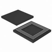
LPC2458FET180,551 NXP Semiconductors, LPC2458FET180,551 Datasheet - Page 31

LPC2458FET180,551
Manufacturer Part Number
LPC2458FET180,551
Description
IC ARM7 MCU FLASH 512K 180TFBGA
Manufacturer
NXP Semiconductors
Series
LPC2400r
Specifications of LPC2458FET180,551
Core Processor
ARM7
Core Size
16/32-Bit
Speed
72MHz
Connectivity
CAN, EBI/EMI, Ethernet, I²C, Microwire, MMC, SPI, SSI, SSP, UART/USART, USB OTG
Peripherals
Brown-out Detect/Reset, DMA, I²S, POR, PWM, WDT
Number Of I /o
136
Program Memory Size
512KB (512K x 8)
Program Memory Type
FLASH
Ram Size
98K x 8
Voltage - Supply (vcc/vdd)
3 V ~ 3.6 V
Data Converters
A/D 8x10b; D/A 1x10b
Oscillator Type
Internal
Operating Temperature
-40°C ~ 85°C
Package / Case
180-TFBGA
Processor Series
LPC24
Core
ARM7TDMI-S
Data Bus Width
32 bit
Data Ram Size
98 KB
Interface Type
CAN, Ethernet, I2C, I2S, IrDA, SPI, SSP, UART, USB
Maximum Clock Frequency
72 MHz
Number Of Programmable I/os
136
Number Of Timers
4
Operating Supply Voltage
3.3 V
Maximum Operating Temperature
+ 85 C
Mounting Style
SMD/SMT
3rd Party Development Tools
MDK-ARM, RL-ARM, ULINK2, SAB-TFBGA180
Minimum Operating Temperature
- 40 C
On-chip Adc
10 bit, 8 Channel
On-chip Dac
10 bit, 1 Channel
Package
180TFBGA
Device Core
ARM7TDMI-S
Family Name
LPC2000
Maximum Speed
72 MHz
For Use With
622-1023 - BOARD SCKT ADAPTER FOR TFBGA180622-1005 - USB IN-CIRCUIT PROG ARM7 LPC2K
Lead Free Status / RoHS Status
Lead free / RoHS Compliant
Eeprom Size
-
Lead Free Status / Rohs Status
Details
Other names
568-4258
935282454551
LPC2458FET180-S
935282454551
LPC2458FET180-S
Available stocks
Company
Part Number
Manufacturer
Quantity
Price
Company:
Part Number:
LPC2458FET180,551
Manufacturer:
MICROCHIP
Quantity:
1 103
Company:
Part Number:
LPC2458FET180,551
Manufacturer:
NXP Semiconductors
Quantity:
10 000
- Current page: 31 of 792
- Download datasheet (5Mb)
NXP Semiconductors
UM10237_4
User manual
3.2 Reset
Table 27.
Reset has four sources on the LPC2400: the RESET pin, the Watchdog Reset, Power On
Reset (POR) and the Brown Out Detection circuit (BOD). The RESET pin is a Schmitt
trigger input pin. Assertion of chip Reset by any source, once the operating voltage attains
a usable level, starts the Wakeup Timer (see description in
this chapter), causing reset to remain asserted until the external Reset is de-asserted, the
oscillator is running, a fixed number of clocks have passed, and the flash controller has
completed its initialization. The reset logic is shown in
Bit Symbol
0
1
2
3
7:4 -
EXTPOLAR0 0
EXTPOLAR1 0
EXTPOLAR2 0
EXTPOLAR3 0
External Interrupt Polarity register (EXTPOLAR - address 0xE01F C14C) bit
description
Value Description
1
1
1
1
-
Rev. 04 — 26 August 2009
EINT0 is low-active or falling-edge sensitive (depending on
EXTMODE0).
EINT0 is high-active or rising-edge sensitive (depending on
EXTMODE0).
EINT1 is low-active or falling-edge sensitive (depending on
EXTMODE1).
EINT1 is high-active or rising-edge sensitive (depending on
EXTMODE1).
EINT2 is low-active or falling-edge sensitive (depending on
EXTMODE2).
EINT2 is high-active or rising-edge sensitive (depending on
EXTMODE2).
EINT3 is low-active or falling-edge sensitive (depending on
EXTMODE3).
EINT3 is high-active or rising-edge sensitive (depending on
EXTMODE3).
Reserved, user software should not write ones to reserved
bits. The value read from a reserved bit is not defined.
Chapter 3: LPC24XX System control
Figure
Section 4–5 “Wakeup timer”
3–10.
UM10237
© NXP B.V. 2009. All rights reserved.
31 of 792
Reset
value
0
0
0
0
NA
in
Related parts for LPC2458FET180,551
Image
Part Number
Description
Manufacturer
Datasheet
Request
R

Part Number:
Description:
NXP Semiconductors designed the LPC2458 microcontroller around a 16-bit/32-bitARM7TDMI-S CPU core with real-time debug interfaces that include both JTAG andembedded trace
Manufacturer:
NXP Semiconductors
Datasheet:
Part Number:
Description:
NXP Semiconductors designed the LPC2420/2460 microcontroller around a 16-bit/32-bitARM7TDMI-S CPU core with real-time debug interfaces that include both JTAG andembedded trace
Manufacturer:
NXP Semiconductors
Datasheet:
Part Number:
Description:
NXP Semiconductors designed the LPC2468 microcontroller around a 16-bit/32-bitARM7TDMI-S CPU core with real-time debug interfaces that include both JTAG andembedded trace
Manufacturer:
NXP Semiconductors
Datasheet:
Part Number:
Description:
NXP Semiconductors designed the LPC2470 microcontroller, powered by theARM7TDMI-S core, to be a highly integrated microcontroller for a wide range ofapplications that require advanced communications and high quality graphic displays
Manufacturer:
NXP Semiconductors
Datasheet:
Part Number:
Description:
NXP Semiconductors designed the LPC2478 microcontroller, powered by theARM7TDMI-S core, to be a highly integrated microcontroller for a wide range ofapplications that require advanced communications and high quality graphic displays
Manufacturer:
NXP Semiconductors
Datasheet:
Part Number:
Description:
The Philips Semiconductors XA (eXtended Architecture) family of 16-bit single-chip microcontrollers is powerful enough to easily handle the requirements of high performance embedded applications, yet inexpensive enough to compete in the market for hi
Manufacturer:
NXP Semiconductors
Datasheet:
Part Number:
Description:
The XA-S3 device is a member of Philips Semiconductors? XA(eXtended Architecture) family of high performance 16-bitsingle-chip microcontrollers
Manufacturer:
NXP Semiconductors
Datasheet:

Part Number:
Description:
The NXP BlueStreak LH75401/LH75411 family consists of two low-cost 16/32-bit System-on-Chip (SoC) devices
Manufacturer:
NXP Semiconductors
Datasheet:

Part Number:
Description:
The NXP LPC3130/3131 combine an 180 MHz ARM926EJ-S CPU core, high-speed USB2
Manufacturer:
NXP Semiconductors
Datasheet:

Part Number:
Description:
The NXP LPC3141 combine a 270 MHz ARM926EJ-S CPU core, High-speed USB 2
Manufacturer:
NXP Semiconductors

Part Number:
Description:
The NXP LPC3143 combine a 270 MHz ARM926EJ-S CPU core, High-speed USB 2
Manufacturer:
NXP Semiconductors

Part Number:
Description:
The NXP LPC3152 combines an 180 MHz ARM926EJ-S CPU core, High-speed USB 2
Manufacturer:
NXP Semiconductors

Part Number:
Description:
The NXP LPC3154 combines an 180 MHz ARM926EJ-S CPU core, High-speed USB 2
Manufacturer:
NXP Semiconductors

Part Number:
Description:
Standard level N-channel enhancement mode Field-Effect Transistor (FET) in a plastic package using NXP High-Performance Automotive (HPA) TrenchMOS technology
Manufacturer:
NXP Semiconductors
Datasheet:


