DK-DEV-4SGX230N Altera, DK-DEV-4SGX230N Datasheet - Page 91
DK-DEV-4SGX230N
Manufacturer Part Number
DK-DEV-4SGX230N
Description
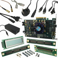
KIT DEVELOPMENT STRATIX IV
Manufacturer
Altera
Series
Stratix® IVr
Type
FPGAr
Datasheets
1.EP4SGX110DF29C3N.pdf
(80 pages)
2.EP4SGX110DF29C3N.pdf
(1154 pages)
3.DK-DEV-4SGX230N.pdf
(2 pages)
4.DK-DEV-4SGX530N.pdf
(57 pages)
Specifications of DK-DEV-4SGX230N
Contents
Development Board, Universal Power Supply, Cables and Software
Silicon Manufacturer
Altera
Core Architecture
FPGA
Core Sub-architecture
Stratix
Silicon Core Number
EP4S
Silicon Family Name
Stratix IV GX
Rohs Compliant
Yes
For Use With/related Products
EP4SGX230K
Lead Free Status / RoHS Status
Lead free / RoHS Compliant
Other names
544-2594
Available stocks
Company
Part Number
Manufacturer
Quantity
Price
Company:

Part Number:
DK-DEV-4SGX230N
Manufacturer:
Altera
Quantity:
135


Chapter 4: DSP Blocks in Stratix IV Devices
Stratix IV DSP Block Resource Descriptions
February 2011 Altera Corporation
A feature of the input register bank is to support a tap delay line. Therefore, the top
leg of the multiplier input (A) can be driven from general routing or from the cascade
chain, as shown in
signals.
Figure 4–7. Input Register of a Half DSP Block
At compile time, you must select whether the A-input comes from general routing or
from the cascade chain. In cascade mode, the dedicated shift outputs from one
multiplier block and directly feeds the input registers of the adjacent multiplier below
it (within the same half DSP block) or the first multiplier in the next half DSP block, to
form an 8-tap shift register chain per DSP Block. The DSP block can increase the
length of the shift register chain by cascading to the lower DSP blocks. The dedicated
shift register chain spans a single column, but you can implement longer shift register
chains requiring multiple columns using the regular FPGA routing resources.
datab_2[17..0]
dataa_3[17..0]
datab_3[17..0]
dataa_1[17..0]
datab_1[17..0]
dataa_2[17..0]
dataa_0[17..0]
datab_0[17..0]
loopback
scanina[17..0]
Figure
4–7.
clock[3..0]
Table 4–9 on page 4–34
ena[3..0]
aclr[3..0]
Register
Delay
scanouta
signa
signb
+/-
+/-
lists the DSP block dynamic
Stratix IV Device Handbook Volume 1
4–11
Related parts for DK-DEV-4SGX230N
Image
Part Number
Description
Manufacturer
Datasheet
Request
R

Part Number:
Description:
KIT DEV ARRIA II GX FPGA 2AGX125
Manufacturer:
Altera
Datasheet:

Part Number:
Description:
KIT DEV CYCLONE III LS EP3CLS200
Manufacturer:
Altera
Datasheet:

Part Number:
Description:
KIT DEV STRATIX IV FPGA 4SE530
Manufacturer:
Altera
Datasheet:

Part Number:
Description:
KIT DEV FPGA 2AGX260 W/6.375G TX
Manufacturer:
Altera
Datasheet:

Part Number:
Description:
KIT DEV MAX V 5M570Z
Manufacturer:
Altera
Datasheet:

Part Number:
Description:
KIT DEV STRATIX V FPGA 5SGXEA7
Manufacturer:
Altera
Datasheet:

Part Number:
Description:
KIT DEVELOPMENT STRATIX III
Manufacturer:
Altera
Datasheet:

Part Number:
Description:
KIT DEV ARRIA GX 1AGX60N
Manufacturer:
Altera
Datasheet:
Part Number:
Description:
KIT STARTER CYCLONE IV GX
Manufacturer:
Altera
Datasheet:
Part Number:
Description:
KIT DEVELOPMENT STRATIX IV
Manufacturer:
Altera
Datasheet:

Part Number:
Description:
CPLD, EP610 Family, ECMOS Process, 300 Gates, 16 Macro Cells, 16 Reg., 16 User I/Os, 5V Supply, 35 Speed Grade, 24DIP
Manufacturer:
Altera Corporation
Datasheet:
Part Number:
Description:
CPLD, EP610 Family, ECMOS Process, 300 Gates, 16 Macro Cells, 16 Reg., 16 User I/Os, 5V Supply, 15 Speed Grade, 24DIP
Manufacturer:
Altera Corporation
Datasheet: