DK-DEV-4SGX230N Altera, DK-DEV-4SGX230N Datasheet - Page 147
DK-DEV-4SGX230N
Manufacturer Part Number
DK-DEV-4SGX230N
Description
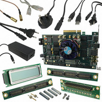
KIT DEVELOPMENT STRATIX IV
Manufacturer
Altera
Series
Stratix® IVr
Type
FPGAr
Datasheets
1.EP4SGX110DF29C3N.pdf
(80 pages)
2.EP4SGX110DF29C3N.pdf
(1154 pages)
3.DK-DEV-4SGX230N.pdf
(2 pages)
4.DK-DEV-4SGX530N.pdf
(57 pages)
Specifications of DK-DEV-4SGX230N
Contents
Development Board, Universal Power Supply, Cables and Software
Silicon Manufacturer
Altera
Core Architecture
FPGA
Core Sub-architecture
Stratix
Silicon Core Number
EP4S
Silicon Family Name
Stratix IV GX
Rohs Compliant
Yes
For Use With/related Products
EP4SGX230K
Lead Free Status / RoHS Status
Lead free / RoHS Compliant
Other names
544-2594
Available stocks
Company
Part Number
Manufacturer
Quantity
Price
Company:

Part Number:
DK-DEV-4SGX230N
Manufacturer:
Altera
Quantity:
135


Chapter 5: Clock Networks and PLLs in Stratix IV Devices
PLLs in Stratix IV Devices
Figure 5–26. ZDB Mode in Stratix IV PLLs
Note to
(1) The bidirectional I/O pin must be assigned to the PLL_<#>_FB_CLKOUT0p pin for left and right PLLs and to the PLL_<#>_FBp_/CLKOUT1 pin for
February 2011 Altera Corporation
top and bottom PLLs.
Figure
5–26:
1
inclk
When using ZDB mode, to avoid signal reflection, do not place board traces on the
bi-directional I/O pin.
Figure 5–27
ZDB mode.
Figure 5–27. Phase Relationship Between the PLL Clocks in ZDB Mode
Note to
(1) The internal PLL clock output can lead or lag the external PLL clock outputs.
External Feedback Mode
In external feedback mode, the external feedback input pin (fbin) is phase-aligned
with the clock input pin, as shown in
remove clock delay and skew between devices. This mode is supported on all
Stratix IV PLLs.
In external feedback mode, the output of the M counter (FBOUT) feeds back to the PLL
fbin input (using a trace on the board) becoming part of the feedback loop. Also, use
one of the dual-purpose external clock outputs as the fbin input pin in this mode.
When using external feedback mode, you must use the same I/O standard on the
input clock, feedback input, and output clocks. Left and right PLLs support this mode
when using single-ended I/O standards only.
÷n
Figure
5–27:
shows an example waveform of the PLL clocks’ phase relationship in
PLL Clock at the
Register Clock Port (1)
PFD
Dedicated PLL
Clock Outputs
PLL Reference
Clock at the
Input Pin
CP/LF
Phase Aligned
VCO
Figure
÷C0
÷C1
÷m
5–28. Aligning these clocks allows you to
fbout
fbin
PLL_<#>_CLKOUT#
PLL_<#>_CLKOUT#
Stratix IV Device Handbook Volume 1
bidirectional
I/O pin (1)
5–31
Related parts for DK-DEV-4SGX230N
Image
Part Number
Description
Manufacturer
Datasheet
Request
R

Part Number:
Description:
KIT DEV ARRIA II GX FPGA 2AGX125
Manufacturer:
Altera
Datasheet:

Part Number:
Description:
KIT DEV CYCLONE III LS EP3CLS200
Manufacturer:
Altera
Datasheet:

Part Number:
Description:
KIT DEV STRATIX IV FPGA 4SE530
Manufacturer:
Altera
Datasheet:

Part Number:
Description:
KIT DEV FPGA 2AGX260 W/6.375G TX
Manufacturer:
Altera
Datasheet:

Part Number:
Description:
KIT DEV MAX V 5M570Z
Manufacturer:
Altera
Datasheet:

Part Number:
Description:
KIT DEV STRATIX V FPGA 5SGXEA7
Manufacturer:
Altera
Datasheet:

Part Number:
Description:
KIT DEVELOPMENT STRATIX III
Manufacturer:
Altera
Datasheet:

Part Number:
Description:
KIT DEV ARRIA GX 1AGX60N
Manufacturer:
Altera
Datasheet:
Part Number:
Description:
KIT STARTER CYCLONE IV GX
Manufacturer:
Altera
Datasheet:
Part Number:
Description:
KIT DEVELOPMENT STRATIX IV
Manufacturer:
Altera
Datasheet:

Part Number:
Description:
CPLD, EP610 Family, ECMOS Process, 300 Gates, 16 Macro Cells, 16 Reg., 16 User I/Os, 5V Supply, 35 Speed Grade, 24DIP
Manufacturer:
Altera Corporation
Datasheet:
Part Number:
Description:
CPLD, EP610 Family, ECMOS Process, 300 Gates, 16 Macro Cells, 16 Reg., 16 User I/Os, 5V Supply, 15 Speed Grade, 24DIP
Manufacturer:
Altera Corporation
Datasheet: