DK-DEV-4SGX230N Altera, DK-DEV-4SGX230N Datasheet - Page 139
DK-DEV-4SGX230N
Manufacturer Part Number
DK-DEV-4SGX230N
Description
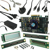
KIT DEVELOPMENT STRATIX IV
Manufacturer
Altera
Series
Stratix® IVr
Type
FPGAr
Datasheets
1.EP4SGX110DF29C3N.pdf
(80 pages)
2.EP4SGX110DF29C3N.pdf
(1154 pages)
3.DK-DEV-4SGX230N.pdf
(2 pages)
4.DK-DEV-4SGX530N.pdf
(57 pages)
Specifications of DK-DEV-4SGX230N
Contents
Development Board, Universal Power Supply, Cables and Software
Silicon Manufacturer
Altera
Core Architecture
FPGA
Core Sub-architecture
Stratix
Silicon Core Number
EP4S
Silicon Family Name
Stratix IV GX
Rohs Compliant
Yes
For Use With/related Products
EP4SGX230K
Lead Free Status / RoHS Status
Lead free / RoHS Compliant
Other names
544-2594
Available stocks
Company
Part Number
Manufacturer
Quantity
Price
Company:

Part Number:
DK-DEV-4SGX230N
Manufacturer:
Altera
Quantity:
135


Chapter 5: Clock Networks and PLLs in Stratix IV Devices
PLLs in Stratix IV Devices
Figure 5–19. Stratix IV PLL Block Diagram
Notes to
(1) The number of post-scale counters is seven for left and right PLLs and ten for top and bottom PLLs.
(2) This is the VCO post-scale counter K.
(3) The FBOUT port is fed by the M counter in Stratix IV PLLs.
February 2011 Altera Corporation
from adjacent PLL
Cascade input
GCLK/RCLK
clock inputs
Dedicated
pfdena
Figure
5–19:
1
4
Figure 5–19
Stratix IV PLL.
You can drive the GCLK or RCLK inputs using an output from another PLL, a
pin-driven GCLK or RCLK, or through a clock control block provided the clock
control block is fed by an output from another PLL or a pin-driven dedicated GCLK
or RCLK. An internally generated global signal or general purpose I/O pin cannot
drive the PLL.
PLL Clock I/O Pins
Each top and bottom PLL supports six clock I/O pins, organized as three pairs of
pins:
■
■
■
inclk0
inclk1
1st pair—two single-ended I/O or one differential I/O
2nd pair—two single-ended I/O or one differential external feedback input
(FBp/FBn)
3rd pair—two single-ended I/O or one differential input
Switchover
Clock
Block
shows a simplified block diagram of the major components of the
÷n
clkswitch
clkbad0
clkbad1
activeclock
PFD
Circuit
Lock
CP
locked
LF
VCO
8
no compensation mode
ZDB, External feedback modes
LVDS Compensation mode
Source Synchronous, normal modes
÷2
(2)
To DPA block on
Left/Right PLLs
/2, /4
8
8
Stratix IV Device Handbook Volume 1
÷C0
÷C1
÷C2
÷C3
÷Cn
÷m
(1)
Casade output
to adjacent PLL
FBIN
DIFFIOCLK network
GCLK/RCLK network
GCLKs
RCLKs
External clock
outputs
DIFFIOCLK from
Left/Right PLLs
LOAD_EN from
Left/Right PLLs
FBOUT (3)
External
memory
interface DLL
5–23
Related parts for DK-DEV-4SGX230N
Image
Part Number
Description
Manufacturer
Datasheet
Request
R

Part Number:
Description:
KIT DEV ARRIA II GX FPGA 2AGX125
Manufacturer:
Altera
Datasheet:

Part Number:
Description:
KIT DEV CYCLONE III LS EP3CLS200
Manufacturer:
Altera
Datasheet:

Part Number:
Description:
KIT DEV STRATIX IV FPGA 4SE530
Manufacturer:
Altera
Datasheet:

Part Number:
Description:
KIT DEV FPGA 2AGX260 W/6.375G TX
Manufacturer:
Altera
Datasheet:

Part Number:
Description:
KIT DEV MAX V 5M570Z
Manufacturer:
Altera
Datasheet:

Part Number:
Description:
KIT DEV STRATIX V FPGA 5SGXEA7
Manufacturer:
Altera
Datasheet:

Part Number:
Description:
KIT DEVELOPMENT STRATIX III
Manufacturer:
Altera
Datasheet:

Part Number:
Description:
KIT DEV ARRIA GX 1AGX60N
Manufacturer:
Altera
Datasheet:
Part Number:
Description:
KIT STARTER CYCLONE IV GX
Manufacturer:
Altera
Datasheet:
Part Number:
Description:
KIT DEVELOPMENT STRATIX IV
Manufacturer:
Altera
Datasheet:

Part Number:
Description:
CPLD, EP610 Family, ECMOS Process, 300 Gates, 16 Macro Cells, 16 Reg., 16 User I/Os, 5V Supply, 35 Speed Grade, 24DIP
Manufacturer:
Altera Corporation
Datasheet:
Part Number:
Description:
CPLD, EP610 Family, ECMOS Process, 300 Gates, 16 Macro Cells, 16 Reg., 16 User I/Os, 5V Supply, 15 Speed Grade, 24DIP
Manufacturer:
Altera Corporation
Datasheet: