DK-DEV-4SGX230N Altera, DK-DEV-4SGX230N Datasheet - Page 156
DK-DEV-4SGX230N
Manufacturer Part Number
DK-DEV-4SGX230N
Description
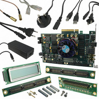
KIT DEVELOPMENT STRATIX IV
Manufacturer
Altera
Series
Stratix® IVr
Type
FPGAr
Datasheets
1.EP4SGX110DF29C3N.pdf
(80 pages)
2.EP4SGX110DF29C3N.pdf
(1154 pages)
3.DK-DEV-4SGX230N.pdf
(2 pages)
4.DK-DEV-4SGX530N.pdf
(57 pages)
Specifications of DK-DEV-4SGX230N
Contents
Development Board, Universal Power Supply, Cables and Software
Silicon Manufacturer
Altera
Core Architecture
FPGA
Core Sub-architecture
Stratix
Silicon Core Number
EP4S
Silicon Family Name
Stratix IV GX
Rohs Compliant
Yes
For Use With/related Products
EP4SGX230K
Lead Free Status / RoHS Status
Lead free / RoHS Compliant
Other names
544-2594
Available stocks
Company
Part Number
Manufacturer
Quantity
Price
Company:

Part Number:
DK-DEV-4SGX230N
Manufacturer:
Altera
Quantity:
135


5–40
Stratix IV Device Handbook Volume 1
In automatic switchover mode, the clkbad[0] and clkbad[1] signals indicate the
status of the two clock inputs. When they are asserted, the clock sense block has
detected that the corresponding clock input has stopped toggling. These two signals
are not valid if the frequency difference between inclk0 and inclk1 is greater than
20%.
The activeclock signal indicates which of the two clock inputs (inclk0 or inclk1) is
being selected as the reference clock to the PLL. When the frequency difference
between the two clock inputs is more than 20%, the activeclock signal is the only
valid status signal.
Figure 5–35
automatic switchover mode. In this example, the inclk0 signal is stuck low. After the
inclk0 signal is stuck at low for approximately two clock cycles, the clock sense
circuitry drives the clkbad[0] signal high. Also, because the reference clock signal is
not toggling, the switchover state machine controls the multiplexer through the
clkswitch signal to switch to the backup clock, inclk1.
Figure 5–35. Automatic Switchover After Loss of Clock Detection
Note to
(1) Switchover is enabled on the falling edge of inclk0 or inclk1, depending on which clock is available. In this figure,
Manual Override
In automatic switchover with manual override mode, you can use the clkswitch
input for user- or system-controlled switch conditions. You can use this mode for
same-frequency switchover, or to switch between inputs of different frequencies. For
example, if inclk0 is 66 MHz and inclk1 is 200 MHz, you must control switchover
using clkswitch because the automatic clock-sense circuitry cannot monitor clock
input (inclk0 and inclk1) frequencies with a frequency difference of more than 100%
(2×). This feature is useful when the clock sources originate from multiple cards on the
backplane, requiring a system-controlled switchover between the frequencies of
operation. You must choose the backup clock frequency and set the m, n, c, and k
counters accordingly so the VCO operates within the recommended operating
frequency range of 600 to 1,600 MHz. The ALTPLL MegaWizard Plug-in Manager
notifies you if a given combination of inclk0 and inclk1 frequencies cannot meet this
requirement.
switchover is enabled on the falling edge of inclk1.
Figure
5–35:
shows an example waveform of the switchover feature when using
activeclock
clkbad0
clkbad1
muxout
inclk0
inclk1
Chapter 5: Clock Networks and PLLs in Stratix IV Devices
(1)
February 2011 Altera Corporation
PLLs in Stratix IV Devices
Related parts for DK-DEV-4SGX230N
Image
Part Number
Description
Manufacturer
Datasheet
Request
R

Part Number:
Description:
KIT DEV ARRIA II GX FPGA 2AGX125
Manufacturer:
Altera
Datasheet:

Part Number:
Description:
KIT DEV CYCLONE III LS EP3CLS200
Manufacturer:
Altera
Datasheet:

Part Number:
Description:
KIT DEV STRATIX IV FPGA 4SE530
Manufacturer:
Altera
Datasheet:

Part Number:
Description:
KIT DEV FPGA 2AGX260 W/6.375G TX
Manufacturer:
Altera
Datasheet:

Part Number:
Description:
KIT DEV MAX V 5M570Z
Manufacturer:
Altera
Datasheet:

Part Number:
Description:
KIT DEV STRATIX V FPGA 5SGXEA7
Manufacturer:
Altera
Datasheet:

Part Number:
Description:
KIT DEVELOPMENT STRATIX III
Manufacturer:
Altera
Datasheet:

Part Number:
Description:
KIT DEV ARRIA GX 1AGX60N
Manufacturer:
Altera
Datasheet:
Part Number:
Description:
KIT STARTER CYCLONE IV GX
Manufacturer:
Altera
Datasheet:
Part Number:
Description:
KIT DEVELOPMENT STRATIX IV
Manufacturer:
Altera
Datasheet:

Part Number:
Description:
CPLD, EP610 Family, ECMOS Process, 300 Gates, 16 Macro Cells, 16 Reg., 16 User I/Os, 5V Supply, 35 Speed Grade, 24DIP
Manufacturer:
Altera Corporation
Datasheet:
Part Number:
Description:
CPLD, EP610 Family, ECMOS Process, 300 Gates, 16 Macro Cells, 16 Reg., 16 User I/Os, 5V Supply, 15 Speed Grade, 24DIP
Manufacturer:
Altera Corporation
Datasheet: