DK-DEV-4SGX230N Altera, DK-DEV-4SGX230N Datasheet - Page 615
DK-DEV-4SGX230N
Manufacturer Part Number
DK-DEV-4SGX230N
Description
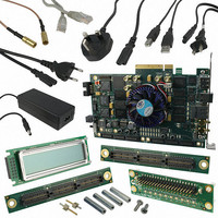
KIT DEVELOPMENT STRATIX IV
Manufacturer
Altera
Series
Stratix® IVr
Type
FPGAr
Datasheets
1.EP4SGX110DF29C3N.pdf
(80 pages)
2.EP4SGX110DF29C3N.pdf
(1154 pages)
3.DK-DEV-4SGX230N.pdf
(2 pages)
4.DK-DEV-4SGX530N.pdf
(57 pages)
Specifications of DK-DEV-4SGX230N
Contents
Development Board, Universal Power Supply, Cables and Software
Silicon Manufacturer
Altera
Core Architecture
FPGA
Core Sub-architecture
Stratix
Silicon Core Number
EP4S
Silicon Family Name
Stratix IV GX
Rohs Compliant
Yes
For Use With/related Products
EP4SGX230K
Lead Free Status / RoHS Status
Lead free / RoHS Compliant
Other names
544-2594
Available stocks
Company
Part Number
Manufacturer
Quantity
Price
Company:

Part Number:
DK-DEV-4SGX230N
Manufacturer:
Altera
Quantity:
135


Chapter 1: Transceiver Architecture in Stratix IV Devices
Transceiver Block Architecture
Figure 1–137. Rate Match Deletion in GIGE Mode
Figure 1–138. Rate Match Insertion in GIGE Mode
February 2011 Altera Corporation
rx_rmfifodatadeleted
rx_rmfifodatainserted
dataout
dataout
datain
datain
In GIGE mode, the rate match FIFO is capable of compensating for up to ±100 PPM
(200 PPM total) difference between the upstream transmitter and the local receiver
reference clock. The GIGE protocol requires the transmitter to send idle ordered sets
/I1/ (/K28.5/D5.6/) and /I2/ (/K28.5/D16.2/) during inter-packet gaps adhering to
the rules listed in the IEEE 802.3 specification.
The rate match operation begins after the synchronization state machine in the word
aligner indicates synchronization is acquired by driving the rx_syncstatus signal
high. The rate matcher deletes or inserts both symbols (/K28.5/ and /D16.2/) of the
/I2/ ordered sets even if it requires deleting only one symbol to prevent the rate
match FIFO from overflowing or under-running. It can insert or delete as many /I2/
ordered sets as necessary to perform the rate match operation.
Two flags, rx_rmfifodatadeleted and rx_rmfifodatainserted, indicating rate match
FIFO deletion and insertion events, respectively, are forwarded to the FPGA fabric.
Both the rx_rmfifodatadeleted and rx_rmfifodatainserted flags are asserted for
two clock cycles for each deleted and inserted /I2/ ordered set, respectively.
Figure 1–137
required to be deleted. Because the rate match FIFO can only delete /I2/ ordered set,
it deletes two /I2/ ordered sets (four symbols deleted).
Figure 1–138
symbol is required to be inserted. Because the rate match FIFO can only delete /I2/
ordered set, it inserts one /I2/ ordered set (two symbols inserted).
For more information, refer to
page
Rate Match FIFO
1–77.
Dx.y
Dx.y
Dx.y
Dx.y
First /I2/ Skip Ordered Set
shows an example of rate match FIFO deletion where three symbols are
shows an example of rate match FIFO insertion in the case where one
First /I2/ Ordered Set
K28.5
K28.5
K28.5
K28.5
D16.2
D16.2
D16.2
D16.2
/I2/ SKIP Symbol Deleted
“Rate Match (Clock Rate Compensation) FIFO” on
Second /I2/ Skip Ordered Set
Second /I2/ Ordered Set
Dx.y
K28.5
K28.5
K28.5
D16.2
D16.2
D16.2
Stratix IV Device Handbook Volume 2: Transceivers
K28.5
K28.5
Third /I2/ Skip Ordered Set
D16.2
D16.2
Dx.y
Dx.y
1–171
Related parts for DK-DEV-4SGX230N
Image
Part Number
Description
Manufacturer
Datasheet
Request
R

Part Number:
Description:
KIT DEV ARRIA II GX FPGA 2AGX125
Manufacturer:
Altera
Datasheet:

Part Number:
Description:
KIT DEV CYCLONE III LS EP3CLS200
Manufacturer:
Altera
Datasheet:

Part Number:
Description:
KIT DEV STRATIX IV FPGA 4SE530
Manufacturer:
Altera
Datasheet:

Part Number:
Description:
KIT DEV FPGA 2AGX260 W/6.375G TX
Manufacturer:
Altera
Datasheet:

Part Number:
Description:
KIT DEV MAX V 5M570Z
Manufacturer:
Altera
Datasheet:

Part Number:
Description:
KIT DEV STRATIX V FPGA 5SGXEA7
Manufacturer:
Altera
Datasheet:

Part Number:
Description:
KIT DEVELOPMENT STRATIX III
Manufacturer:
Altera
Datasheet:

Part Number:
Description:
KIT DEV ARRIA GX 1AGX60N
Manufacturer:
Altera
Datasheet:
Part Number:
Description:
KIT STARTER CYCLONE IV GX
Manufacturer:
Altera
Datasheet:
Part Number:
Description:
KIT DEVELOPMENT STRATIX IV
Manufacturer:
Altera
Datasheet:

Part Number:
Description:
CPLD, EP610 Family, ECMOS Process, 300 Gates, 16 Macro Cells, 16 Reg., 16 User I/Os, 5V Supply, 35 Speed Grade, 24DIP
Manufacturer:
Altera Corporation
Datasheet:
Part Number:
Description:
CPLD, EP610 Family, ECMOS Process, 300 Gates, 16 Macro Cells, 16 Reg., 16 User I/Os, 5V Supply, 15 Speed Grade, 24DIP
Manufacturer:
Altera Corporation
Datasheet: