DK-DEV-4SGX230N Altera, DK-DEV-4SGX230N Datasheet - Page 60
DK-DEV-4SGX230N
Manufacturer Part Number
DK-DEV-4SGX230N
Description
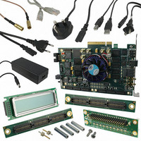
KIT DEVELOPMENT STRATIX IV
Manufacturer
Altera
Series
Stratix® IVr
Type
FPGAr
Datasheets
1.EP4SGX110DF29C3N.pdf
(80 pages)
2.EP4SGX110DF29C3N.pdf
(1154 pages)
3.DK-DEV-4SGX230N.pdf
(2 pages)
4.DK-DEV-4SGX530N.pdf
(57 pages)
Specifications of DK-DEV-4SGX230N
Contents
Development Board, Universal Power Supply, Cables and Software
Silicon Manufacturer
Altera
Core Architecture
FPGA
Core Sub-architecture
Stratix
Silicon Core Number
EP4S
Silicon Family Name
Stratix IV GX
Rohs Compliant
Yes
For Use With/related Products
EP4SGX230K
Lead Free Status / RoHS Status
Lead free / RoHS Compliant
Other names
544-2594
Available stocks
Company
Part Number
Manufacturer
Quantity
Price
Company:

Part Number:
DK-DEV-4SGX230N
Manufacturer:
Altera
Quantity:
135


3–4
Figure 3–1. Byte Enable Functional Waveform
Stratix IV Device Handbook Volume 1
current data: q (asynch)
don't care: q (asynch)
contents at a0
contents at a1
contents at a2
Packed Mode Support
address
byteena
inclock
1
wren
data
You cannot use the byte enable feature when using the error correction coding (ECC)
feature on M144K blocks.
Figure 3–1
control the operations of the RAM blocks.
When a byte-enable bit is de-asserted during a write cycle, the corresponding data
byte output can appear as either a “don’t care” value or the current data at that
location. The output value for the masked byte is controllable using the Quartus II
software. When a byte-enable bit is asserted during a write cycle, the corresponding
data byte output also depends on the setting chosen in the Quartus II software.
Stratix IV M9K and M144K blocks support packed mode. The packed mode feature
packs two independent single-port RAMs into one memory block. The Quartus II
software automatically implements packed mode where appropriate by placing the
physical RAM block into true dual-port mode and using the MSB of the address to
distinguish between the two logical RAMs. The size of each independent single-port
RAM must not exceed half of the target block size.
XXXX
XX
an
FFFF
doutn
doutn
FFFF
shows how the write enable (wren) and byte enable (byteena) signals
10
a0
FFFF
ABXX
ABFF
ABCD
01
a1
XXCD
FFCD
Chapter 3: TriMatrix Embedded Memory Blocks in Stratix IV Devices
11
a2
ABCD
ABCD
ABFF
a0
FFCD
ABFF
ABFF
ABCD
a1
February 2011 Altera Corporation
XXXX
XX
FFCD
FFCD
a2
ABCD
ABCD
Overview
Related parts for DK-DEV-4SGX230N
Image
Part Number
Description
Manufacturer
Datasheet
Request
R

Part Number:
Description:
KIT DEV ARRIA II GX FPGA 2AGX125
Manufacturer:
Altera
Datasheet:

Part Number:
Description:
KIT DEV CYCLONE III LS EP3CLS200
Manufacturer:
Altera
Datasheet:

Part Number:
Description:
KIT DEV STRATIX IV FPGA 4SE530
Manufacturer:
Altera
Datasheet:

Part Number:
Description:
KIT DEV FPGA 2AGX260 W/6.375G TX
Manufacturer:
Altera
Datasheet:

Part Number:
Description:
KIT DEV MAX V 5M570Z
Manufacturer:
Altera
Datasheet:

Part Number:
Description:
KIT DEV STRATIX V FPGA 5SGXEA7
Manufacturer:
Altera
Datasheet:

Part Number:
Description:
KIT DEVELOPMENT STRATIX III
Manufacturer:
Altera
Datasheet:

Part Number:
Description:
KIT DEV ARRIA GX 1AGX60N
Manufacturer:
Altera
Datasheet:
Part Number:
Description:
KIT STARTER CYCLONE IV GX
Manufacturer:
Altera
Datasheet:
Part Number:
Description:
KIT DEVELOPMENT STRATIX IV
Manufacturer:
Altera
Datasheet:

Part Number:
Description:
CPLD, EP610 Family, ECMOS Process, 300 Gates, 16 Macro Cells, 16 Reg., 16 User I/Os, 5V Supply, 35 Speed Grade, 24DIP
Manufacturer:
Altera Corporation
Datasheet:
Part Number:
Description:
CPLD, EP610 Family, ECMOS Process, 300 Gates, 16 Macro Cells, 16 Reg., 16 User I/Os, 5V Supply, 15 Speed Grade, 24DIP
Manufacturer:
Altera Corporation
Datasheet: