DK-DEV-4SGX230N Altera, DK-DEV-4SGX230N Datasheet - Page 367
DK-DEV-4SGX230N
Manufacturer Part Number
DK-DEV-4SGX230N
Description
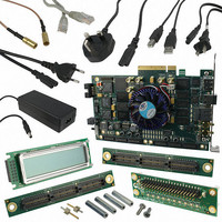
KIT DEVELOPMENT STRATIX IV
Manufacturer
Altera
Series
Stratix® IVr
Type
FPGAr
Datasheets
1.EP4SGX110DF29C3N.pdf
(80 pages)
2.EP4SGX110DF29C3N.pdf
(1154 pages)
3.DK-DEV-4SGX230N.pdf
(2 pages)
4.DK-DEV-4SGX530N.pdf
(57 pages)
Specifications of DK-DEV-4SGX230N
Contents
Development Board, Universal Power Supply, Cables and Software
Silicon Manufacturer
Altera
Core Architecture
FPGA
Core Sub-architecture
Stratix
Silicon Core Number
EP4S
Silicon Family Name
Stratix IV GX
Rohs Compliant
Yes
For Use With/related Products
EP4SGX230K
Lead Free Status / RoHS Status
Lead free / RoHS Compliant
Other names
544-2594
Available stocks
Company
Part Number
Manufacturer
Quantity
Price
Company:

Part Number:
DK-DEV-4SGX230N
Manufacturer:
Altera
Quantity:
135


Chapter 10: Configuration, Design Security, and Remote System Upgrades in Stratix IV Devices
Passive Serial Configuration
Figure 10–14. PS Configuration Using a USB Blaster, EthernetBlaster, MasterBlaster, ByteBlaster II, or ByteBlasterMV
Cable
Notes to
(1) Connect the pull-up resistor to the same supply voltage (V
(2) You only need the pull-up resistors on DATA0 and DCLK if the download cable is the only configuration scheme used on your board. This ensures
(3) Pin 6 of the header is a V
April 2011 Altera Corporation
EthernetBlaster cable.
that DATA0 and DCLK are not left floating after configuration. For example, if you are also using a configuration device, you do not need the
pull-up resistors on DATA0 and DCLK.
this value, refer to the
this pin is a no connect.
Figure
10–14:
1
MasterBlaster Serial/USB Communications Cable User
The configuration cycle consists of three stages—reset, configuration, and
initialization. While nCONFIG or nSTATUS are low, the device is in reset. To initiate
configuration in this scheme, the download cable generates a low-to-high transition
on the nCONFIG pin.
To begin configuration, power the V
banks where the configuration pins reside) to the appropriate voltage levels.
When nCONFIG goes high, the device comes out of reset and releases the open-drain
nSTATUS pin, which is then pulled high by an external 10-kΩ pull-up resistor. After
nSTATUS is released, the device is ready to receive configuration data and the
configuration stage begins. The programming hardware or download cable then
places the configuration data one bit at a time on the device’s DATA0 pin. The
configuration data is clocked into the target device until CONF_DONE goes high. The
CONF_DONE pin must have an external 10-kΩ pull-up resistor for the device to initialize.
When using a download cable, setting the Auto-restart configuration after error
option does not affect the configuration cycle because you must manually restart
configuration in the Quartus II software when an error occurs. Additionally, the
Enable user-supplied start-up clock (CLKUSR) option has no affect on the device
initialization because this option is disabled in the .sof when programming the device
using the Quartus II programmer and download cable. Therefore, if you turn on the
CLKUSR option, you do not need to provide a clock on CLKUSR when you are
configuring the device with the Quartus II programmer and a download cable.
Figure 10–14
EthernetBlaster, MasterBlaster, ByteBlaster II, or ByteBlasterMV cable.
IO
V
reference voltage for the MasterBlaster output driver. V
CCPGM
(2)
(1)
10
V
kΩ
CCPGM
(2)
10
kΩ
(1)
V
CCPGM
shows PS configuration for Stratix IV devices using a USB Blaster,
10
(1)
kΩ
V CCPGM
GND
GND
CCPGM
MSEL2
MSEL1
MSEL0
nCE
DCLK
DATA0
nCONFIG
) as the USB Blaster, MasterBlaster (VIO pin), ByteBlaster II, ByteBlasterMV, or
Stratix IV Device
CONF_DONE
nSTATUS
nCEO
CC
Guide. In the USB-Blaster, ByteBlaster II, and ByteBlasterMV cable,
, V
N.C.
IO
CCIO
V
CCPGM
must match the device’s V
, V
(1) V
10
kΩ
CCPGM
CCPGM
Pin 1
10
(1)
kΩ
10-Pin Male Header
Download Cable
, and V
(PS Mode)
Shield
GND
V
V
CCPGM
IO
Stratix IV Device Handbook Volume 1
(3)
GND
CCPD
CCPGM
(1)
. For more information about
voltages (for the
10–33
Related parts for DK-DEV-4SGX230N
Image
Part Number
Description
Manufacturer
Datasheet
Request
R

Part Number:
Description:
KIT DEV ARRIA II GX FPGA 2AGX125
Manufacturer:
Altera
Datasheet:

Part Number:
Description:
KIT DEV CYCLONE III LS EP3CLS200
Manufacturer:
Altera
Datasheet:

Part Number:
Description:
KIT DEV STRATIX IV FPGA 4SE530
Manufacturer:
Altera
Datasheet:

Part Number:
Description:
KIT DEV FPGA 2AGX260 W/6.375G TX
Manufacturer:
Altera
Datasheet:

Part Number:
Description:
KIT DEV MAX V 5M570Z
Manufacturer:
Altera
Datasheet:

Part Number:
Description:
KIT DEV STRATIX V FPGA 5SGXEA7
Manufacturer:
Altera
Datasheet:

Part Number:
Description:
KIT DEVELOPMENT STRATIX III
Manufacturer:
Altera
Datasheet:

Part Number:
Description:
KIT DEV ARRIA GX 1AGX60N
Manufacturer:
Altera
Datasheet:
Part Number:
Description:
KIT STARTER CYCLONE IV GX
Manufacturer:
Altera
Datasheet:
Part Number:
Description:
KIT DEVELOPMENT STRATIX IV
Manufacturer:
Altera
Datasheet:

Part Number:
Description:
CPLD, EP610 Family, ECMOS Process, 300 Gates, 16 Macro Cells, 16 Reg., 16 User I/Os, 5V Supply, 35 Speed Grade, 24DIP
Manufacturer:
Altera Corporation
Datasheet:
Part Number:
Description:
CPLD, EP610 Family, ECMOS Process, 300 Gates, 16 Macro Cells, 16 Reg., 16 User I/Os, 5V Supply, 15 Speed Grade, 24DIP
Manufacturer:
Altera Corporation
Datasheet: