DK-DEV-4SGX230N Altera, DK-DEV-4SGX230N Datasheet - Page 266
DK-DEV-4SGX230N
Manufacturer Part Number
DK-DEV-4SGX230N
Description
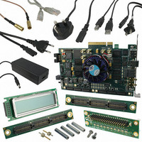
KIT DEVELOPMENT STRATIX IV
Manufacturer
Altera
Series
Stratix® IVr
Type
FPGAr
Datasheets
1.EP4SGX110DF29C3N.pdf
(80 pages)
2.EP4SGX110DF29C3N.pdf
(1154 pages)
3.DK-DEV-4SGX230N.pdf
(2 pages)
4.DK-DEV-4SGX530N.pdf
(57 pages)
Specifications of DK-DEV-4SGX230N
Contents
Development Board, Universal Power Supply, Cables and Software
Silicon Manufacturer
Altera
Core Architecture
FPGA
Core Sub-architecture
Stratix
Silicon Core Number
EP4S
Silicon Family Name
Stratix IV GX
Rohs Compliant
Yes
For Use With/related Products
EP4SGX230K
Lead Free Status / RoHS Status
Lead free / RoHS Compliant
Other names
544-2594
Available stocks
Company
Part Number
Manufacturer
Quantity
Price
Company:

Part Number:
DK-DEV-4SGX230N
Manufacturer:
Altera
Quantity:
135


7–46
Figure 7–26. Avoiding Glitch on a Non-Consecutive Read Burst Waveform
Stratix IV Device Handbook Volume 1
Postamble Enable
dqsenable
DQS
DQS Postamble Circuitry
For external memory interfaces that use a bidirectional read strobe such as in DDR3,
DDR2, and DDR SDRAM, the DQS signal is low before going to or coming from a
high-impedance state. The state in which DQS is low, just after a high-impedance
state, is called the preamble; the state in which DQS is low, just before it returns to a
high-impedance state, is called the postamble. There are preamble and postamble
specifications for both read and write operations in DDR3, DDR2, and DDR SDRAM.
The DQS postamble circuitry ensures that data is not lost if there is noise on the DQS
line during the end of a read operation that occurs while DQS is in a postamble state.
Stratix IV devices have dedicated postamble registers that you can control to ground
the shifted DQS signal used to clock the DQ input registers at the end of a read
operation. This ensures that any glitches on the DQS input signals during the end of a
read operation that occurs while DQS is in a postamble state do not affect the DQ IOE
registers.
In addition to the dedicated postamble register, Stratix IV devices also have an HDR
block inside the postamble enable circuitry. Use these registers if the controller is
running at half the frequency of the I/Os.
Using the HDR block as the first stage capture register in the postamble enable
circuitry block is optional. The HDR block is clocked by the half-rate
resynchronization clock, which is the output of the I/O clock divider circuit (shown in
Figure 7–31 on page
that is used to avoid postamble glitches from a previous read burst on a
non-consecutive read burst. This scheme allows a half-a-clock cycle latency for
dqsenable assertion and zero latency for dqsenable de-assertion, as shown in
Figure
7–26.
7–50). There is an AND gate after the postamble register outputs
Chapter 7: External Memory Interfaces in Stratix IV Devices
Postamble
Stratix IV External Memory Interface Features
Postamble glitch
February 2011 Altera Corporation
Preamble
Delayed by
1/2T logic
Related parts for DK-DEV-4SGX230N
Image
Part Number
Description
Manufacturer
Datasheet
Request
R

Part Number:
Description:
KIT DEV ARRIA II GX FPGA 2AGX125
Manufacturer:
Altera
Datasheet:

Part Number:
Description:
KIT DEV CYCLONE III LS EP3CLS200
Manufacturer:
Altera
Datasheet:

Part Number:
Description:
KIT DEV STRATIX IV FPGA 4SE530
Manufacturer:
Altera
Datasheet:

Part Number:
Description:
KIT DEV FPGA 2AGX260 W/6.375G TX
Manufacturer:
Altera
Datasheet:

Part Number:
Description:
KIT DEV MAX V 5M570Z
Manufacturer:
Altera
Datasheet:

Part Number:
Description:
KIT DEV STRATIX V FPGA 5SGXEA7
Manufacturer:
Altera
Datasheet:

Part Number:
Description:
KIT DEVELOPMENT STRATIX III
Manufacturer:
Altera
Datasheet:

Part Number:
Description:
KIT DEV ARRIA GX 1AGX60N
Manufacturer:
Altera
Datasheet:
Part Number:
Description:
KIT STARTER CYCLONE IV GX
Manufacturer:
Altera
Datasheet:
Part Number:
Description:
KIT DEVELOPMENT STRATIX IV
Manufacturer:
Altera
Datasheet:

Part Number:
Description:
CPLD, EP610 Family, ECMOS Process, 300 Gates, 16 Macro Cells, 16 Reg., 16 User I/Os, 5V Supply, 35 Speed Grade, 24DIP
Manufacturer:
Altera Corporation
Datasheet:
Part Number:
Description:
CPLD, EP610 Family, ECMOS Process, 300 Gates, 16 Macro Cells, 16 Reg., 16 User I/Os, 5V Supply, 15 Speed Grade, 24DIP
Manufacturer:
Altera Corporation
Datasheet: