DK-DEV-4SGX230N Altera, DK-DEV-4SGX230N Datasheet - Page 660
DK-DEV-4SGX230N
Manufacturer Part Number
DK-DEV-4SGX230N
Description
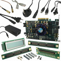
KIT DEVELOPMENT STRATIX IV
Manufacturer
Altera
Series
Stratix® IVr
Type
FPGAr
Datasheets
1.EP4SGX110DF29C3N.pdf
(80 pages)
2.EP4SGX110DF29C3N.pdf
(1154 pages)
3.DK-DEV-4SGX230N.pdf
(2 pages)
4.DK-DEV-4SGX530N.pdf
(57 pages)
Specifications of DK-DEV-4SGX230N
Contents
Development Board, Universal Power Supply, Cables and Software
Silicon Manufacturer
Altera
Core Architecture
FPGA
Core Sub-architecture
Stratix
Silicon Core Number
EP4S
Silicon Family Name
Stratix IV GX
Rohs Compliant
Yes
For Use With/related Products
EP4SGX230K
Lead Free Status / RoHS Status
Lead free / RoHS Compliant
Other names
544-2594
Available stocks
Company
Part Number
Manufacturer
Quantity
Price
Company:

Part Number:
DK-DEV-4SGX230N
Manufacturer:
Altera
Quantity:
135


1–216
Table 1–74. Stratix IV GX and GT ALTGX Megafunction Ports: Receiver Ports (Part 5 of 7)
Stratix IV Device Handbook Volume 2: Transceivers
rx_runningdisp
Byte Ordering Block
rx_enabyteord
rx_
byteorderalignstatus
Receiver Phase Compensation FIFO
rx_dataout
rx_clkout
Port Name
Output
Output
Output
Output
Output
Input/
Input
coreclkout for
coreclkout for
coreclkout for
Synchronous to
Synchronous to
Synchronous to
rx_clkout or
rx_clkout or
rx_clkout or
rx_clkout for
bonded modes
rx_clkout for
bonded modes
rx_clkout for
bonded modes
Asynchronous
Clock Domain
coreclkout.
coreclkout.
coreclkout.
non-bonded
non-bonded
non-bonded
Clock signal
modes.
modes.
modes.
signal
8B/10B running disparity indicator.
■
■
■
■
Enable byte ordering control.
■
■
Byte ordering status indicator.
■
■
Parallel data output from the receiver to the
FPGA fabric.
■
Recovered clock from the receiver channel.
■
Available in configurations with the 8B/10B
decoder.
A high level—the data on the rx_dataout
port was received with a negative running
disparity.
A low level—the data on the rx_dataout
port was received with a positive running
disparity.
Channel Width:
8—rx_runningdisp = 1
16—rx_runningdisp = 2
32—rx_runningdisp = 4
Available in configurations with the byte
ordering block enabled. The byte ordering
block is rising-edge sensitive to this signal.
A low-to-high transition triggers the byte
ordering block to restart the byte ordering
operation.
Available in configurations with the byte
ordering block enabled.
A high level—the byte ordering block has
detected the programmed byte ordering
pattern in the LSByte of the received data
from the byte deserializer.
The bus width depends on the channel width
multiplied by the number of channels per
instance.
Available only when the rate match FIFO is
not used in the receiver datapath.
Chapter 1: Transceiver Architecture in Stratix IV Devices
Description
February 2011 Altera Corporation
Transceiver Port Lists
Channel
Channel
Channel
Channel
Channel
Scope
Related parts for DK-DEV-4SGX230N
Image
Part Number
Description
Manufacturer
Datasheet
Request
R

Part Number:
Description:
KIT DEV ARRIA II GX FPGA 2AGX125
Manufacturer:
Altera
Datasheet:

Part Number:
Description:
KIT DEV CYCLONE III LS EP3CLS200
Manufacturer:
Altera
Datasheet:

Part Number:
Description:
KIT DEV STRATIX IV FPGA 4SE530
Manufacturer:
Altera
Datasheet:

Part Number:
Description:
KIT DEV FPGA 2AGX260 W/6.375G TX
Manufacturer:
Altera
Datasheet:

Part Number:
Description:
KIT DEV MAX V 5M570Z
Manufacturer:
Altera
Datasheet:

Part Number:
Description:
KIT DEV STRATIX V FPGA 5SGXEA7
Manufacturer:
Altera
Datasheet:

Part Number:
Description:
KIT DEVELOPMENT STRATIX III
Manufacturer:
Altera
Datasheet:

Part Number:
Description:
KIT DEV ARRIA GX 1AGX60N
Manufacturer:
Altera
Datasheet:
Part Number:
Description:
KIT STARTER CYCLONE IV GX
Manufacturer:
Altera
Datasheet:
Part Number:
Description:
KIT DEVELOPMENT STRATIX IV
Manufacturer:
Altera
Datasheet:

Part Number:
Description:
CPLD, EP610 Family, ECMOS Process, 300 Gates, 16 Macro Cells, 16 Reg., 16 User I/Os, 5V Supply, 35 Speed Grade, 24DIP
Manufacturer:
Altera Corporation
Datasheet:
Part Number:
Description:
CPLD, EP610 Family, ECMOS Process, 300 Gates, 16 Macro Cells, 16 Reg., 16 User I/Os, 5V Supply, 15 Speed Grade, 24DIP
Manufacturer:
Altera Corporation
Datasheet: