DK-DEV-4SGX230N Altera, DK-DEV-4SGX230N Datasheet - Page 307
DK-DEV-4SGX230N
Manufacturer Part Number
DK-DEV-4SGX230N
Description
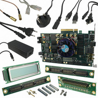
KIT DEVELOPMENT STRATIX IV
Manufacturer
Altera
Series
Stratix® IVr
Type
FPGAr
Datasheets
1.EP4SGX110DF29C3N.pdf
(80 pages)
2.EP4SGX110DF29C3N.pdf
(1154 pages)
3.DK-DEV-4SGX230N.pdf
(2 pages)
4.DK-DEV-4SGX530N.pdf
(57 pages)
Specifications of DK-DEV-4SGX230N
Contents
Development Board, Universal Power Supply, Cables and Software
Silicon Manufacturer
Altera
Core Architecture
FPGA
Core Sub-architecture
Stratix
Silicon Core Number
EP4S
Silicon Family Name
Stratix IV GX
Rohs Compliant
Yes
For Use With/related Products
EP4SGX230K
Lead Free Status / RoHS Status
Lead free / RoHS Compliant
Other names
544-2594
Available stocks
Company
Part Number
Manufacturer
Quantity
Price
Company:

Part Number:
DK-DEV-4SGX230N
Manufacturer:
Altera
Quantity:
135


Chapter 8: High-Speed Differential I/O Interfaces and DPA in Stratix IV Devices
Left and Right PLLs (PLL_Lx and PLL_Rx)
Figure 8–22. Phase Relationship for External PLL Interface Signals
Left and Right PLLs (PLL_Lx and PLL_Rx)
February 2011 Altera Corporation
(internal PLL clk)
phase shift)
phase shift)
phase shift)
Serial data
c0 (-180
VCO clk
c1 (288
c2 (-18
inclk0
f
D1
The
data are edge aligned. Introducing a phase shift of –180° to sampling clock (c0)
ensures that the input data is center-aligned with respect to the c0, as shown in
Figure
The Stratix IV device family contains up to eight left and right PLLs with up to four
PLLs located on the left side and four on the right side of the device. The left PLLs can
support high-speed differential I/O banks on the left side; the right PLLs can support
high-speed differential I/O banks on the right side of the device. The high-speed
differential I/O receiver and transmitter channels use these left and right PLLs to
generate the parallel clocks (rx_outclock and tx_outclock) and high-speed clocks
(diffioclk).
Figure 8–2 on page 8–3
right PLLs for Stratix IV E, GT, and GX devices. The PLL VCO operates at the clock
frequency of the data rate. Clock switchover and dynamic reconfiguration are allowed
using the left and right PLL in high-speed differential I/O support mode.
For more information, refer to the
Equation 8–1
8–22.
D2
D3
calculations for phase shift assume that the input clock and serial
and
D4
Figure 8–3 on page 8–4
D5
Clock Network and PLLs in Stratix IV Devices
D6
D7
show the locations of the left and
D8
Stratix IV Device Handbook Volume 1
D9
D10
chapter.
8–29
Related parts for DK-DEV-4SGX230N
Image
Part Number
Description
Manufacturer
Datasheet
Request
R

Part Number:
Description:
KIT DEV ARRIA II GX FPGA 2AGX125
Manufacturer:
Altera
Datasheet:

Part Number:
Description:
KIT DEV CYCLONE III LS EP3CLS200
Manufacturer:
Altera
Datasheet:

Part Number:
Description:
KIT DEV STRATIX IV FPGA 4SE530
Manufacturer:
Altera
Datasheet:

Part Number:
Description:
KIT DEV FPGA 2AGX260 W/6.375G TX
Manufacturer:
Altera
Datasheet:

Part Number:
Description:
KIT DEV MAX V 5M570Z
Manufacturer:
Altera
Datasheet:

Part Number:
Description:
KIT DEV STRATIX V FPGA 5SGXEA7
Manufacturer:
Altera
Datasheet:

Part Number:
Description:
KIT DEVELOPMENT STRATIX III
Manufacturer:
Altera
Datasheet:

Part Number:
Description:
KIT DEV ARRIA GX 1AGX60N
Manufacturer:
Altera
Datasheet:
Part Number:
Description:
KIT STARTER CYCLONE IV GX
Manufacturer:
Altera
Datasheet:
Part Number:
Description:
KIT DEVELOPMENT STRATIX IV
Manufacturer:
Altera
Datasheet:

Part Number:
Description:
CPLD, EP610 Family, ECMOS Process, 300 Gates, 16 Macro Cells, 16 Reg., 16 User I/Os, 5V Supply, 35 Speed Grade, 24DIP
Manufacturer:
Altera Corporation
Datasheet:
Part Number:
Description:
CPLD, EP610 Family, ECMOS Process, 300 Gates, 16 Macro Cells, 16 Reg., 16 User I/Os, 5V Supply, 15 Speed Grade, 24DIP
Manufacturer:
Altera Corporation
Datasheet: