DK-DEV-4SGX230N Altera, DK-DEV-4SGX230N Datasheet - Page 732
DK-DEV-4SGX230N
Manufacturer Part Number
DK-DEV-4SGX230N
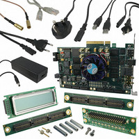
Description
KIT DEVELOPMENT STRATIX IV
Manufacturer
Altera
Series
Stratix® IVr
Type
FPGAr
Datasheets
1.EP4SGX110DF29C3N.pdf
(80 pages)
2.EP4SGX110DF29C3N.pdf
(1154 pages)
3.DK-DEV-4SGX230N.pdf
(2 pages)
4.DK-DEV-4SGX530N.pdf
(57 pages)
Specifications of DK-DEV-4SGX230N
Contents
Development Board, Universal Power Supply, Cables and Software
Silicon Manufacturer
Altera
Core Architecture
FPGA
Core Sub-architecture
Stratix
Silicon Core Number
EP4S
Silicon Family Name
Stratix IV GX
Rohs Compliant
Yes
For Use With/related Products
EP4SGX230K
Lead Free Status / RoHS Status
Lead free / RoHS Compliant
Other names
544-2594
Available stocks
Company
Part Number
Manufacturer
Quantity
Price
Company:

Part Number:
DK-DEV-4SGX230N
Manufacturer:
Altera
Quantity:
135


2–60
Table 2–15. Transmitter Phase Compensation FIFO Read Clocks
Stratix IV Device Handbook Volume 2: Transceivers
Non-Bonded Channel
Configuration
×4 Bonded Channel
Configuration
×8 Bonded Channel
Configuration
Configuration
1
1
1
Table 2–15
Quartus II software selects in various configurations.
To ensure that you understand the 0 PPM clock driver rule, the Quartus II software
expects the following set of user assignments whenever you use the tx_coreclk port
to drive the transmitter phase compensation FIFO write clock:
■
Failing to make this assignment correctly when using the tx_coreclk port results in a
Quartus II compilation error.
The GXB 0 PPM core clock setting allows the following clock drivers to drive the
tx_coreclk ports:
■
■
■
■
■
The Quartus II software does not allow gated clocks or clocks generated in FPGA
logic to drive the tx_coreclk ports.
Because the GXB 0 PPM core clock setting allows the FPGA CLK input pins and
transceiver refclk pins as the clock driver, the Quartus II compiler cannot determine
if there is a 0 PPM difference between the FIFO write clock and read clock for each
channel.
You must ensure that the clock driver for all connected tx_coreclk ports has a 0 PPM
difference with respect to the FIFO read clock in those channels.
Parallel transmitter PCS clock from the local
clock divider in the associated channel
(tx_clkout)
Low-speed parallel clock from the CMU0
clock divider of the associated transceiver
block (coreclkout)
Low-speed parallel clock from the CMU0
clock divider of the master transceiver block
(coreclkout from master transceiver block)
GXB 0 PPM Core Clock Setting
tx_clkout in non-bonded channel configurations
coreclkout in bonded channel configurations
FPGA_CLK input pins
Transceiver refclk pins
Clock output from left and right and top and bottom PLLs (PLL_L, PLL_R, and
PLL_T, PLL_B)
Without Byte Serializer
lists the transmitter phase compensation FIFO read clocks that the
Transmitter Phase Compensation FIFO Read Clock
Divide-by-two version of the parallel transmitter PCS
clock from the local clock divider in the associated
channel (tx_clkout)
Divide-by-two version of the low-speed parallel
clock from the CMU0 clock divider of the associated
transceiver block (coreclkout)
Divide-by-two version of the low-speed parallel
clock from the CMU0 clock divider of the master
transceiver block (coreclkout from master
transceiver block)
Chapter 2: Transceiver Clocking in Stratix IV Devices
With Byte Serializer
FPGA Fabric-Transceiver Interface Clocking
February 2011 Altera Corporation
Related parts for DK-DEV-4SGX230N
Image
Part Number
Description
Manufacturer
Datasheet
Request
R

Part Number:
Description:
KIT DEV ARRIA II GX FPGA 2AGX125
Manufacturer:
Altera
Datasheet:

Part Number:
Description:
KIT DEV CYCLONE III LS EP3CLS200
Manufacturer:
Altera
Datasheet:

Part Number:
Description:
KIT DEV STRATIX IV FPGA 4SE530
Manufacturer:
Altera
Datasheet:

Part Number:
Description:
KIT DEV FPGA 2AGX260 W/6.375G TX
Manufacturer:
Altera
Datasheet:

Part Number:
Description:
KIT DEV MAX V 5M570Z
Manufacturer:
Altera
Datasheet:

Part Number:
Description:
KIT DEV STRATIX V FPGA 5SGXEA7
Manufacturer:
Altera
Datasheet:

Part Number:
Description:
KIT DEVELOPMENT STRATIX III
Manufacturer:
Altera
Datasheet:

Part Number:
Description:
KIT DEV ARRIA GX 1AGX60N
Manufacturer:
Altera
Datasheet:
Part Number:
Description:
KIT STARTER CYCLONE IV GX
Manufacturer:
Altera
Datasheet:
Part Number:
Description:
KIT DEVELOPMENT STRATIX IV
Manufacturer:
Altera
Datasheet:

Part Number:
Description:
CPLD, EP610 Family, ECMOS Process, 300 Gates, 16 Macro Cells, 16 Reg., 16 User I/Os, 5V Supply, 35 Speed Grade, 24DIP
Manufacturer:
Altera Corporation
Datasheet:
Part Number:
Description:
CPLD, EP610 Family, ECMOS Process, 300 Gates, 16 Macro Cells, 16 Reg., 16 User I/Os, 5V Supply, 15 Speed Grade, 24DIP
Manufacturer:
Altera Corporation
Datasheet: