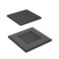
HD6417720BP133BV Renesas Electronics America, HD6417720BP133BV Datasheet - Page 523

HD6417720BP133BV
Manufacturer Part Number
HD6417720BP133BV
Description
SH3-DSP, WITH USB AND LCDC, PB-F
Manufacturer
Renesas Electronics America
Series
SuperH® SH7700r
Datasheet
1.R8A77210C133BAV.pdf
(1478 pages)
Specifications of HD6417720BP133BV
Core Processor
SH-3 DSP
Core Size
32-Bit
Speed
133MHz
Connectivity
FIFO, I²C, IrDA, MMC, SCI, SD, SIO, SIM, USB
Peripherals
DMA, LCD, POR, WDT
Number Of I /o
117
Program Memory Type
ROMless
Ram Size
16K x 8
Voltage - Supply (vcc/vdd)
1.4 V ~ 1.6 V
Data Converters
A/D 4x10b; D/A 2x8b
Oscillator Type
Internal
Operating Temperature
-20°C ~ 75°C
Package / Case
256-BGA
Lead Free Status / RoHS Status
Lead free / RoHS Compliant
Eeprom Size
-
Program Memory Size
-
- Current page: 523 of 1478
- Download datasheet (10Mb)
SH7720 Group, SH7721 Group
11.4
The CPG has the following registers. Refer to section 37, List of Registers, for more details on the
addresses and access size of these registers.
• Frequency control register (FRQCR)
• USBH/USBF clock control register (UCLKCR)
11.4.1
The frequency control register (FRQCR) is a 16-bit readable/writable register used to specify
whether a clock is output from the CKIO pin, the frequency multiplication ratio of PLL circuit 1,
and the frequency division ratio of the internal clock and the peripheral clock.
Only word access can be used on the FRQCR register. FRQCR is initialized by a power-on reset,
but not initialized by a power-on reset at the WDT overflow. FRQCR retains its value in a manual
reset and in standby mode.
The write values to bits 14, 13, 11, 10, 7, 6, and 3 should always be 0.
R01UH0083EJ0400 Rev. 4.00
Sep 21, 2010
Bit
15
14, 13 ⎯
Bit Name
PLL2EN
Register Descriptions
Frequency Control Register (FRQCR)
Initial
Value
0
All 0
R/W
R/W
R
Description
PLL2 Enable
PLL2EN specifies whether make the PLL circuit 2 ON in
clock operating mode 7.
PLL circuit 2 is ON in clock operating modes other than
mode 7 regardless of the PLL2EN setting.
0: PLL circuit 2 is OFF
1: PLL circuit 2 is ON
Reserved
These bits are always read as 0. The write value should
always be 0.
Section 11 Clock Pulse Generator (CPG)
Page 463 of 1414
Related parts for HD6417720BP133BV
Image
Part Number
Description
Manufacturer
Datasheet
Request
R

Part Number:
Description:
KIT STARTER FOR M16C/29
Manufacturer:
Renesas Electronics America
Datasheet:

Part Number:
Description:
KIT STARTER FOR R8C/2D
Manufacturer:
Renesas Electronics America
Datasheet:

Part Number:
Description:
R0K33062P STARTER KIT
Manufacturer:
Renesas Electronics America
Datasheet:

Part Number:
Description:
KIT STARTER FOR R8C/23 E8A
Manufacturer:
Renesas Electronics America
Datasheet:

Part Number:
Description:
KIT STARTER FOR R8C/25
Manufacturer:
Renesas Electronics America
Datasheet:

Part Number:
Description:
KIT STARTER H8S2456 SHARPE DSPLY
Manufacturer:
Renesas Electronics America
Datasheet:

Part Number:
Description:
KIT STARTER FOR R8C38C
Manufacturer:
Renesas Electronics America
Datasheet:

Part Number:
Description:
KIT STARTER FOR R8C35C
Manufacturer:
Renesas Electronics America
Datasheet:

Part Number:
Description:
KIT STARTER FOR R8CL3AC+LCD APPS
Manufacturer:
Renesas Electronics America
Datasheet:

Part Number:
Description:
KIT STARTER FOR RX610
Manufacturer:
Renesas Electronics America
Datasheet:

Part Number:
Description:
KIT STARTER FOR R32C/118
Manufacturer:
Renesas Electronics America
Datasheet:

Part Number:
Description:
KIT DEV RSK-R8C/26-29
Manufacturer:
Renesas Electronics America
Datasheet:

Part Number:
Description:
KIT STARTER FOR SH7124
Manufacturer:
Renesas Electronics America
Datasheet:

Part Number:
Description:
KIT STARTER FOR H8SX/1622
Manufacturer:
Renesas Electronics America
Datasheet:

Part Number:
Description:
KIT DEV FOR SH7203
Manufacturer:
Renesas Electronics America
Datasheet:


