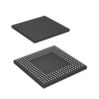
HD6417720BP133BV Renesas Electronics America, HD6417720BP133BV Datasheet - Page 428

HD6417720BP133BV
Manufacturer Part Number
HD6417720BP133BV
Description
SH3-DSP, WITH USB AND LCDC, PB-F
Manufacturer
Renesas Electronics America
Series
SuperH® SH7700r
Datasheet
1.R8A77210C133BAV.pdf
(1478 pages)
Specifications of HD6417720BP133BV
Core Processor
SH-3 DSP
Core Size
32-Bit
Speed
133MHz
Connectivity
FIFO, I²C, IrDA, MMC, SCI, SD, SIO, SIM, USB
Peripherals
DMA, LCD, POR, WDT
Number Of I /o
117
Program Memory Type
ROMless
Ram Size
16K x 8
Voltage - Supply (vcc/vdd)
1.4 V ~ 1.6 V
Data Converters
A/D 4x10b; D/A 2x8b
Oscillator Type
Internal
Operating Temperature
-20°C ~ 75°C
Package / Case
256-BGA
Lead Free Status / RoHS Status
Lead free / RoHS Compliant
Eeprom Size
-
Program Memory Size
-
- Current page: 428 of 1478
- Download datasheet (10Mb)
Section 9 Bus State Controller (BSC)
When bank active mode is set, if only accesses to the respective banks in the area 3 space are
considered, as long as accesses to the same row address continue, the operation starts with the
cycle in figure 9.19 or 9.22, followed by repetition of the cycle in figure 9.20 or 9.23. An access to
a different area during this time has no effect. If there is an access to a different row address in the
bank active state, after this is detected the bus cycle in figure 9.21 or 9.24 is executed instead of
that in figure 9.20 or 9.23. In bank active mode, too, all banks become inactive after a refresh
cycle or after the bus is released as the result of bus arbitration.
Page 368 of 1414
A12/A11*
D31 to D0
A25 to A0
DACKn*
RD/WR
DQMxx
CKIO
RAS
CAS
CSn
BS
Figure 9.19 Burst Read Timing (No Auto-Precharge)
1
2
Notes:
1. Address pin to be connected to the A10 pin of SDRAM.
2. The waveform for DACKn is when active low is specified.
Tr
Tc1
Td1
Tc2
Td2
Tc3
Td3
Tc4
Td4
SH7720 Group, SH7721 Group
Tde
R01UH0083EJ0400 Rev. 4.00
Sep 21, 2010
Related parts for HD6417720BP133BV
Image
Part Number
Description
Manufacturer
Datasheet
Request
R

Part Number:
Description:
KIT STARTER FOR M16C/29
Manufacturer:
Renesas Electronics America
Datasheet:

Part Number:
Description:
KIT STARTER FOR R8C/2D
Manufacturer:
Renesas Electronics America
Datasheet:

Part Number:
Description:
R0K33062P STARTER KIT
Manufacturer:
Renesas Electronics America
Datasheet:

Part Number:
Description:
KIT STARTER FOR R8C/23 E8A
Manufacturer:
Renesas Electronics America
Datasheet:

Part Number:
Description:
KIT STARTER FOR R8C/25
Manufacturer:
Renesas Electronics America
Datasheet:

Part Number:
Description:
KIT STARTER H8S2456 SHARPE DSPLY
Manufacturer:
Renesas Electronics America
Datasheet:

Part Number:
Description:
KIT STARTER FOR R8C38C
Manufacturer:
Renesas Electronics America
Datasheet:

Part Number:
Description:
KIT STARTER FOR R8C35C
Manufacturer:
Renesas Electronics America
Datasheet:

Part Number:
Description:
KIT STARTER FOR R8CL3AC+LCD APPS
Manufacturer:
Renesas Electronics America
Datasheet:

Part Number:
Description:
KIT STARTER FOR RX610
Manufacturer:
Renesas Electronics America
Datasheet:

Part Number:
Description:
KIT STARTER FOR R32C/118
Manufacturer:
Renesas Electronics America
Datasheet:

Part Number:
Description:
KIT DEV RSK-R8C/26-29
Manufacturer:
Renesas Electronics America
Datasheet:

Part Number:
Description:
KIT STARTER FOR SH7124
Manufacturer:
Renesas Electronics America
Datasheet:

Part Number:
Description:
KIT STARTER FOR H8SX/1622
Manufacturer:
Renesas Electronics America
Datasheet:

Part Number:
Description:
KIT DEV FOR SH7203
Manufacturer:
Renesas Electronics America
Datasheet:


