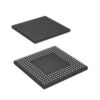
HD6417720BP133BV Renesas Electronics America, HD6417720BP133BV Datasheet - Page 146

HD6417720BP133BV
Manufacturer Part Number
HD6417720BP133BV
Description
SH3-DSP, WITH USB AND LCDC, PB-F
Manufacturer
Renesas Electronics America
Series
SuperH® SH7700r
Datasheet
1.R8A77210C133BAV.pdf
(1478 pages)
Specifications of HD6417720BP133BV
Core Processor
SH-3 DSP
Core Size
32-Bit
Speed
133MHz
Connectivity
FIFO, I²C, IrDA, MMC, SCI, SD, SIO, SIM, USB
Peripherals
DMA, LCD, POR, WDT
Number Of I /o
117
Program Memory Type
ROMless
Ram Size
16K x 8
Voltage - Supply (vcc/vdd)
1.4 V ~ 1.6 V
Data Converters
A/D 4x10b; D/A 2x8b
Oscillator Type
Internal
Operating Temperature
-20°C ~ 75°C
Package / Case
256-BGA
Lead Free Status / RoHS Status
Lead free / RoHS Compliant
Eeprom Size
-
Program Memory Size
-
- Current page: 146 of 1478
- Download datasheet (10Mb)
Section 3 DSP Operating Unit
(2)
The repeat start register (RS) holds the start address of a loop repeat module that is controlled by
the repeat function. This register can be accessed in DSP mode. At reset, the initial value of this
register is undefined. This register is not affected in the exception handling state.
(3)
The repeat end register (RE) holds the end address of a loop repeat module that is controlled by
the repeat function. This register can be accessed in DSP mode. At reset, this register is initialized
to 0. This register is not affected in the exception handling state.
(4)
The modulo register stores the modulo end address and modulo start address for modulo
addressing in upper and lower 16 bits. The upper and lower 16 bits of the modulo register are
referred to as the ME register and MS register, respectively. This register can be accessed in DSP
mode. At reset, the initial value of this register is undefined. This register is not affected in the
exception handling state.
The above registers can be accessed by the control register load instruction (LDC) and store
instruction (STC). Note that the LDC and STC instructions for the RS, RE, and MOD registers can
be used only in privileged DSP mode and user DSP mode. The LDC and STC instruction for the
SR register can be executed only when the MD bit is set to 1 or in user DSP mode. Note, however,
that the LDC and STC instructions can modify only the RC11 to RC0, RF1 to RF0, DMX, and
DMY bits in the SR, as described below.
• In user mode, if the LCD and STC instructions are used for the RS, an illegal instruction
• In privileged and privileged DSP modes, all SR bits can be modified.
• In user DSP mode, the SR can be read by the STC instruction.
• In user DSP mode, the LDC instruction can be issued to the SR but only the DSP extension
Page 86 of 1414
exception occurs.
bits can be modified.
Repeat Start Register (RS)
Repeat End Register (RE)
Modulo Register (MOD)
SH7720 Group, SH7721 Group
R01UH0083EJ0400 Rev. 4.00
Sep 21, 2010
Related parts for HD6417720BP133BV
Image
Part Number
Description
Manufacturer
Datasheet
Request
R

Part Number:
Description:
KIT STARTER FOR M16C/29
Manufacturer:
Renesas Electronics America
Datasheet:

Part Number:
Description:
KIT STARTER FOR R8C/2D
Manufacturer:
Renesas Electronics America
Datasheet:

Part Number:
Description:
R0K33062P STARTER KIT
Manufacturer:
Renesas Electronics America
Datasheet:

Part Number:
Description:
KIT STARTER FOR R8C/23 E8A
Manufacturer:
Renesas Electronics America
Datasheet:

Part Number:
Description:
KIT STARTER FOR R8C/25
Manufacturer:
Renesas Electronics America
Datasheet:

Part Number:
Description:
KIT STARTER H8S2456 SHARPE DSPLY
Manufacturer:
Renesas Electronics America
Datasheet:

Part Number:
Description:
KIT STARTER FOR R8C38C
Manufacturer:
Renesas Electronics America
Datasheet:

Part Number:
Description:
KIT STARTER FOR R8C35C
Manufacturer:
Renesas Electronics America
Datasheet:

Part Number:
Description:
KIT STARTER FOR R8CL3AC+LCD APPS
Manufacturer:
Renesas Electronics America
Datasheet:

Part Number:
Description:
KIT STARTER FOR RX610
Manufacturer:
Renesas Electronics America
Datasheet:

Part Number:
Description:
KIT STARTER FOR R32C/118
Manufacturer:
Renesas Electronics America
Datasheet:

Part Number:
Description:
KIT DEV RSK-R8C/26-29
Manufacturer:
Renesas Electronics America
Datasheet:

Part Number:
Description:
KIT STARTER FOR SH7124
Manufacturer:
Renesas Electronics America
Datasheet:

Part Number:
Description:
KIT STARTER FOR H8SX/1622
Manufacturer:
Renesas Electronics America
Datasheet:

Part Number:
Description:
KIT DEV FOR SH7203
Manufacturer:
Renesas Electronics America
Datasheet:


