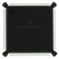
MC68302EH20C Freescale Semiconductor, MC68302EH20C Datasheet - Page 92

MC68302EH20C
Manufacturer Part Number
MC68302EH20C
Description
IC MPU MULTI-PROTOCOL 132-PQFP
Manufacturer
Freescale Semiconductor
Datasheets
1.MC68302AG20C.pdf
(4 pages)
2.MC68302AG20C.pdf
(2 pages)
3.MC68302AG20C.pdf
(13 pages)
4.MC68302EH20C.pdf
(481 pages)
Specifications of MC68302EH20C
Processor Type
M683xx 32-Bit
Speed
20MHz
Voltage
5V
Mounting Type
Surface Mount
Package / Case
132-MQFP, 132-PQFP
Family Name
M68000
Device Core
ColdFire
Device Core Size
32b
Frequency (max)
20MHz
Instruction Set Architecture
RISC
Supply Voltage 1 (typ)
5V
Operating Temp Range
0C to 70C
Operating Temperature Classification
Commercial
Mounting
Surface Mount
Pin Count
132
Package Type
PQFP
Lead Free Status / RoHS Status
Lead free / RoHS Compliant
Features
-
Lead Free Status / Rohs Status
Compliant
Available stocks
Company
Part Number
Manufacturer
Quantity
Price
Company:
Part Number:
MC68302EH20C
Manufacturer:
Freescale Semiconductor
Quantity:
10 000
Part Number:
MC68302EH20C
Manufacturer:
FREESCALE
Quantity:
20 000
Company:
Part Number:
MC68302EH20CB1
Manufacturer:
Freescale Semiconductor
Quantity:
10 000
Company:
Part Number:
MC68302EH20CR2
Manufacturer:
Freescale Semiconductor
Quantity:
10 000
- MC68302AG20C PDF datasheet
- MC68302AG20C PDF datasheet #2
- MC68302AG20C PDF datasheet #3
- MC68302EH20C PDF datasheet #4
- Current page: 92 of 481
- Download datasheet (2Mb)
System Integration Block (SIB)
15
1
0
REFERENCE VALUE
EN
3.5.3.3 Software Watchdog Counter (WCN)
WCN, a 16-bit up-counter, appears as a memory-mapped register and may be read at any
time. Clearing EN in WRR causes the counter to be reset and disables the count operation.
A read cycle to WCN causes the current value of the timer to be read. When working in
MC68008 mode (BUSW is low), reading the high byte of WCN will latch the low byte into a
temporary register. When reading the low byte, the temporary register value is read. Read-
ing the timer does not affect the counting operation.
A write cycle to WCN causes the counter and prescaler to be reset. In the MC68008 mode
(BUSW is low), a write cycle to either the high or low byte resets the counter and the pres-
caler. A write cycle should be executed on a regular basis so that the watchdog timer is nev-
er allowed to reach the reference value during normal program operation.
3.6 EXTERNAL CHIP-SELECT SIGNALS AND WAIT-STATE LOGIC
The MC68302 provides a set of four programmable chip-select signals. Each chip-select
signal has an identical internal structure. For each memory area, the user may also define
an internally generated cycle termination signal (DTACK). This feature eliminates board
space that would be necessary for cycle termination logic.
The four chip-select signals allow four different classes of memory to be used: e.g., high-
speed static RAM, slower dynamic RAM, EPROM, and nonvolatile RAM. If more than four
chip selects are required, additional chip selects may be decoded externally, as on the
MC68000.
The chip-select block diagram is shown in Figure 3-9.
The chip-select logic is active for memory cycles generated by internal bus masters
(M68000 core, IDMA, SDMA, DRAM refresh) or external bus masters. These signals are
driven externally on the falling edge of AS and are valid shortly after AS goes low.
For each chip select, the user programs the block size by choosing the starting address in
the base register and the length in the option register. The starting address must be on a
block boundary. Thus, an 8K block size must begin on an 8K address boundary, and a 64K
block size must begin on a 64K address boundary, etc.
For a given chip-select block, the user may also choose 1) whether the chip-select block
should be considered as read-only, write-only, or read/write, 2) whether the chip-select
block should be active on only one particular function code signal combination or for all func-
tion codes, and 3) whether a DTACK should be automatically generated for this chip-select
block, and after how many wait states.
3-42
MC68302 USER’S MANUAL
MOTOROLA
Related parts for MC68302EH20C
Image
Part Number
Description
Manufacturer
Datasheet
Request
R
Part Number:
Description:
Manufacturer:
Freescale Semiconductor, Inc
Datasheet:

Part Number:
Description:
MC68302 Configuring the Chip Selects on the MC68302
Manufacturer:
Motorola / Freescale Semiconductor

Part Number:
Description:
MC68302 Design Concept - Expanding Interrupts on the MC68302
Manufacturer:
Motorola / Freescale Semiconductor

Part Number:
Description:
MC68302 MC68302 Adapting a WAN Controller to a LAN Environment
Manufacturer:
Motorola / Freescale Semiconductor

Part Number:
Description:
MC68302 EKB Applications - Power Measurements on the MC68302
Manufacturer:
Motorola / Freescale Semiconductor

Part Number:
Description:
MC68302 Interfacing the MC68020 to a Slave MC68302
Manufacturer:
Motorola / Freescale Semiconductor

Part Number:
Description:
MC68302 MC68302 Software Performance
Manufacturer:
Motorola / Freescale Semiconductor

Part Number:
Description:
MC68302 Evaluating EDX on the ADS302
Manufacturer:
Motorola / Freescale Semiconductor

Part Number:
Description:
MC68302 Design Advisory #1 - MC68SC302 Passive ISDN Protocol Engine
Manufacturer:
Motorola / Freescale Semiconductor

Part Number:
Description:
MC68302, MC68360, and MPC860 Characteristics and Design Notes for Crystal Feedback Oscillators
Manufacturer:
Motorola / Freescale Semiconductor
Part Number:
Description:
Mc68302 Integrated Multi-protocol Processor
Manufacturer:
Freescale Semiconductor, Inc
Datasheet:
Part Number:
Description:
Manufacturer:
Freescale Semiconductor, Inc
Datasheet:
Part Number:
Description:
Manufacturer:
Freescale Semiconductor, Inc
Datasheet:
Part Number:
Description:
Manufacturer:
Freescale Semiconductor, Inc
Datasheet:
Part Number:
Description:
Manufacturer:
Freescale Semiconductor, Inc
Datasheet:


