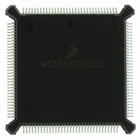
MC68302EH20C Freescale Semiconductor, MC68302EH20C Datasheet - Page 467

MC68302EH20C
Manufacturer Part Number
MC68302EH20C
Description
IC MPU MULTI-PROTOCOL 132-PQFP
Manufacturer
Freescale Semiconductor
Datasheets
1.MC68302AG20C.pdf
(4 pages)
2.MC68302AG20C.pdf
(2 pages)
3.MC68302AG20C.pdf
(13 pages)
4.MC68302EH20C.pdf
(481 pages)
Specifications of MC68302EH20C
Processor Type
M683xx 32-Bit
Speed
20MHz
Voltage
5V
Mounting Type
Surface Mount
Package / Case
132-MQFP, 132-PQFP
Family Name
M68000
Device Core
ColdFire
Device Core Size
32b
Frequency (max)
20MHz
Instruction Set Architecture
RISC
Supply Voltage 1 (typ)
5V
Operating Temp Range
0C to 70C
Operating Temperature Classification
Commercial
Mounting
Surface Mount
Pin Count
132
Package Type
PQFP
Lead Free Status / RoHS Status
Lead free / RoHS Compliant
Features
-
Lead Free Status / Rohs Status
Compliant
Available stocks
Company
Part Number
Manufacturer
Quantity
Price
Company:
Part Number:
MC68302EH20C
Manufacturer:
Freescale Semiconductor
Quantity:
10 000
Part Number:
MC68302EH20C
Manufacturer:
FREESCALE
Quantity:
20 000
Company:
Part Number:
MC68302EH20CB1
Manufacturer:
Freescale Semiconductor
Quantity:
10 000
Company:
Part Number:
MC68302EH20CR2
Manufacturer:
Freescale Semiconductor
Quantity:
10 000
- MC68302AG20C PDF datasheet
- MC68302AG20C PDF datasheet #2
- MC68302AG20C PDF datasheet #3
- MC68302EH20C PDF datasheet #4
- Current page: 467 of 481
- Download datasheet (2Mb)
MOTOROLA
17. Function Code, lnitialize, Reset
18. Function Code, External Bus Master
19. BAR, Write
20. DRAM Refresh
21. Watchdog Timer
22. Underrun, Overrun, Clock Lines, Schmitt-Triggers
does not correctly “equate” locations in parameter RAM to intended addresses. A sim-
ple typo in an assembler EQU or a C #DEFlNE directive can cause 1) the intended
parameter not to be set and 2) another parameter to be set to a wrong value.
To use IDMA, SDMA, and/or DRAM refresh, their corresponding function code regis-
ters MUST be initialized. Setting the function codes in these registers to “111” will pre-
vent the MC68302 chip selects from asserting. Failure to initialize these registers often
results in their function codes having the value “111”, since these registers are in dual-
port RAM and do not have predefined values upon a total system reset.
When an external bus master is using the chip selects on the MC68302 with the ex-
ternal master's external memory accesses, make sure that the external bus master
drives the function code lines to something other than “111". If the function code lines
are driven or left floating to “111”, the external cycle will be interpreted by the MC68302
as an interrupt acknowledge cycle, and the chip selects will not be asserted during the
cycle.
The BAR MUST BE written by an instruction following a total system reset of the
MC68302 since this register resides in the MC68302, not in the memory. It is not suf-
ficient or required for the EPROM on the target board to have the desired BAR value
stored in the EPROM location $0F2 (the address of BAR). When using an emulator, a
symptom of this problem can be that the code works in the emulator overlay memory,
but not on the target.
When using the DRAM refresh unit, one cannot refresh locations $0F0–0FF of an ex-
ternal DRAM if an MC68302 chip select is used to select that DRAM. Locations $0F0–
0FF are designated as the reserved area of the IMP that contains the BAR and SCR,
and chip selects will not activate on accesses to these addresses. The remedy is sim-
ply to use a different DRAM refresh starting address besides $0. Also note that the
DRAM refresh access is a byte read, not a word read.
If the MC68302 watchdog timer is never turned off or refreshed, an unexpected inter-
rupt at level 4 can occur. Also, an unexpected RESET can occur if the WDOG pin is
externally connected to HALT and RESET. The solution is to disable the watchdog tim-
er after reset. Note that the watchdog timer is not related to the hardware watchdog,
which is a completely separate unit that monitors bus activity.
If a transmit underrun or a receive overrun is reported but the data rates are too slow
to suggest an actual underrun or overrun, the problem may be in the clock lines.
Glitched or badly ringing clocks (on the TCLK or RCLK pins) can cause SCCs to enter
either of the above error states. Even though Schmitt-triggers are implemented on the
IMP clocks lines, a very slow rise/fall time coupled with a large amount of noise on the
lines can override the hysteresis protection and affect the ability of the SCC to correctly
sample and clock data. Internal clocks generated by the IMP do not cause this prob-
lem.
MC68360 USER’S MANUAL
Design Checklist
F-3
Related parts for MC68302EH20C
Image
Part Number
Description
Manufacturer
Datasheet
Request
R
Part Number:
Description:
Manufacturer:
Freescale Semiconductor, Inc
Datasheet:

Part Number:
Description:
MC68302 Configuring the Chip Selects on the MC68302
Manufacturer:
Motorola / Freescale Semiconductor

Part Number:
Description:
MC68302 Design Concept - Expanding Interrupts on the MC68302
Manufacturer:
Motorola / Freescale Semiconductor

Part Number:
Description:
MC68302 MC68302 Adapting a WAN Controller to a LAN Environment
Manufacturer:
Motorola / Freescale Semiconductor

Part Number:
Description:
MC68302 EKB Applications - Power Measurements on the MC68302
Manufacturer:
Motorola / Freescale Semiconductor

Part Number:
Description:
MC68302 Interfacing the MC68020 to a Slave MC68302
Manufacturer:
Motorola / Freescale Semiconductor

Part Number:
Description:
MC68302 MC68302 Software Performance
Manufacturer:
Motorola / Freescale Semiconductor

Part Number:
Description:
MC68302 Evaluating EDX on the ADS302
Manufacturer:
Motorola / Freescale Semiconductor

Part Number:
Description:
MC68302 Design Advisory #1 - MC68SC302 Passive ISDN Protocol Engine
Manufacturer:
Motorola / Freescale Semiconductor

Part Number:
Description:
MC68302, MC68360, and MPC860 Characteristics and Design Notes for Crystal Feedback Oscillators
Manufacturer:
Motorola / Freescale Semiconductor
Part Number:
Description:
Mc68302 Integrated Multi-protocol Processor
Manufacturer:
Freescale Semiconductor, Inc
Datasheet:
Part Number:
Description:
Manufacturer:
Freescale Semiconductor, Inc
Datasheet:
Part Number:
Description:
Manufacturer:
Freescale Semiconductor, Inc
Datasheet:
Part Number:
Description:
Manufacturer:
Freescale Semiconductor, Inc
Datasheet:
Part Number:
Description:
Manufacturer:
Freescale Semiconductor, Inc
Datasheet:


